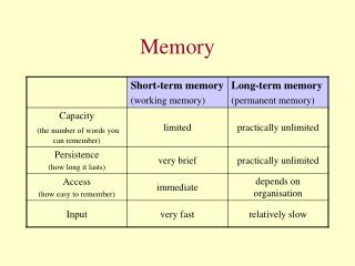
Memory
Memory. Read only memory (ROM) – nonvolatile Data remains when power is turned off, data are written into the ROM during its fabrication at the factory PROM- P rogrammable ROM . Can be programmed by user but this can only be done once EPROM – erasable programmable ROM

Memory
E N D
Presentation Transcript
Memory • Read only memory (ROM) – nonvolatile • Data remains when power is turned off, data are written into the ROM during its fabrication at the factory • PROM- Programmable ROM. Can be programmed by user but this can only be done once • EPROM – erasable programmable ROM • Contents of EPROM can be erased by exposing it to ultraviolet light • EEPROM – Electrical Erasable PROM (your USB memory stick)
Exercise • There is a BIOS in your computer, what kind of memory is it?
Block diagram of a ROM ROM interface – address input, data output, /CE – chip enable, /OE – output enable (for READ operation)
Memory Read Operation • To read a ROM, we need to issue the proper address • There is a delay between address inputs and data outputs • The access time (tACC), chip enable time (tCE), and chip deselect time (tDF) are important timing properties • You need these information for developing a real computer system
Timing parameters • The access time – delay occurs before data stored at the addressed location are stable at the outputs (ie how long it takes to access data). The microprocessor must wait for tACC before reading the data
ROM read operation • Access time is regarded as address to output delay. Typical value is 250ns • tCE – represents the Chip Enable to output delay, usually this is equal to access time • Deselect time – amount of time the device takes for data outputs to return to high-Z state after /OE becomes inactive
Read operation tAA=access time tCO= chip select to output delay tHZ = deselect to output float
Question • A normal 8086 read cycle takes 4 clocks • For a system with a 8MHz clock • Now you are required to develop the memory system for the computer which of the following devices will you use? • Tacc = 0.125us $100 • Tacc = 0.2us $50 • Tacc = 0.4us $20
Configuration of ROM for 8-bit bus How the circuit operates?
EEPROM – electrical Erasable ROM • Data stored in an EEPROM can be erased electrically • Example inside the AduC832 (or 8051) microcontroller, there are 64KBytes of EEPROM
Programming the EPROM • In an erased EPROM, all cells hold logic 1 • Vpp is in logic 1 for data to be read from EPROM • Vpp is ON (eg Vpp = 25V for 2716 EPROM) for programming mode (writing) • 2716 is a 2Kx8 EPROM • To write data to the EPROM a 25V signal is needed so an external device is necessary
Modern EEPROM Charges in the floating gate represent the data Control gate blocked out data = 0 http://www.siliconfareast.com/flash-memory.htm
FLASH EEPROM • http://electronics.howstuffworks.com/flash-memory.htm
Random access memory (RAM) • Data can be read as well as written into the memory chip • Static ram (SRAM) – data remains valid as long as the power is ON • Dynamic RAM (DRAM) – needs to periodically restore (recharge) the data in each storage location by addressing them • If storage nodes are not recharged at regular intervals of time, data would be lost. This process is called refreshing
A static RAM The two inverters are cross-connected to form a latch. The latch is connected to two bit lines by transistors T1 and T2. These transistors act as switches that can be opened or closed under control of the word line. When the word line is at ground level, the transistors are turned off and the latch retains its state. Example, if the logic value at point X is 1 and at point Y is 0, this state is maintained as long as the signal on the word line is at ground level.
SRAM circuit To control RAM: CE – chip enable OE – output enable (for read operation) WE – write enable (for write operation) From decoding logic
Write-cycle for SRAM • To write, we must produce the signal in proper order • Minimum duration of a write cycle is tWC (write cycle time ) • Address must remain stable during the whole cycle • Chip enable (CE) signal becomes active • The Write Enable (WE) will be active after the address setup time tAS elapses
RAM write operation • Data should now ready and must be valid for tDW (data valid to end of write) • Data should remain valid (tDH) after the write • A short recovery period (tWR) takes place after /WE returns to 1 before the write cycle is complete (address is removed)
Read Cycle • Read cycle for RAM is similar to the ROM • Minimum duration of a read cycle is tRC (read cycle time) • Address must remain stable during the whole cycle • Chip enable becomes active • The Enable(s) (CE) will be active after the address is stable • Data should now ready • Data should remain valid after the OE and CE have been removed
Read Cycle CO – time between Valid data and chip enable OE – time between Valid data and output enable
DRAM • DRAM has a higher density • Cost less • Consume less power • Take up less space • We can get 64Mx1, 128Mx1 modules
DRAM structure Needs to periodically restore (recharge) the data in each storage location by addressing them because the data is stored in the form of a charge on a capacitor as shown in the circuit. To store information in this cell, transistor T is turned on and an appropriate voltage is applied to the bit line. This causes a known amount of charge to be stored in the capacitor.
DRAM • After the transistor is turned off, the charge remains stored in the capacitor, but not for long. • The capacitor begins to discharge. During a Read operation, the transistor in a selected cell is turned on. • A sense amplifier connected to the bit line detects whether the charge stored in the capacitor is above or below the threshold value. • If the charge is above the threshold, the sense amplifier drives the bit line to the full voltage representing the logic value 1. If the sense amplifier detects that the charge is below the threshold then it pulls the bit line to ground level to discharge the capacitor fully.
DRAM • If storage nodes are not recharged at regular intervals of time, data would be lost. This process is called refreshing.
DRAM • An example of a DRAM – 2164B • It is a 64K-bit (64Kx1) device with only 16 pins • To address 64K address, requires 16-bit address line • 16-bit address is divided into two separate parts: 8-bit row address, and 8-bit column address. And these are time-multiplexed
DRAM-2164B Address bus is time multiplexed RAS – row address strobe CAS – column address strobe
Addressing the DRAM • The row address is first applied • /RAS is pulsed to ‘0’ to latch the address into the device • The column address is applied and /CAS strobed to ‘0’ • If RAS is left at ‘0’ after the row address is latched inside the device, the address is maintained within the device
DRAM organization Column ROW
DRAM • Data cells along the selected row can be accessed by simply supplying successive column addresses • This is called page mode accesses • (How many bits are there in a row?) • Advantage - faster access of memory is achieved
Refreshing the DRAM • The DRAM must be refreshed every 2ms • Refreshing is achieved by cycling through the row addresses (i.e. generating all the row address) • During refreshing, /CAS is at logic ‘1’ and no data are output
Example 416800 DRAM • The 416800 DRAM is 2Mx8 device and the data is parallel (8-bit) but address is multiplexed divided into ROW and Column. • In order to access 2M memory locations, it takes 21 address bits. In the device, the address lines are multiplexed into: 12 address lines for row address and column address is only 9-bit. • The refresh must be done in every 64ms.
32Mx8 DRAM 16Kx16K array Each row has 2K bytes data To select a row needs 14 bits To select a column 11 bits
Address Decoding • Address decoding is required because many memory chips are used by a computer system • At each memory read/write only a number of chips is used • Decoding mechanism is used to guarantee that the proper chips are selected • Certainly, capacity of modern memory device is large (GB!!) so decoding may not be necessary but if you consider the development of SSD then decoding will become necessary if a SSD is 250G then you still need to use more than 1 memory device • Decoding is necessary inside the memory chip
Address decoding • To design, first determine the number of chips required • Then determine how many address lines are needed for the decoding purpose • Example if 4 chips are used then you need 2 address lines for decoding
Example For 8086 system, max. 1M bytes of memory Now we use 4 256Kx8 memory chip. Note: Even addresses memory locations should be in the same chip Odd addresses memory locations should be in the same chip So the 4 memory chips will be divided into Even and Odd group (two chips per group) Only consider the even group, since the chip is only 256K so the Memory locations stored by one chip is from 00000 to 7FFFF (with only the even locations) The other chip holds 80000 to FFFFF (only the even locations)
Example Odd Even Address 80000 to FFFFF Address 00000 to 7FFFF Now if the address issued is 12345H which memory chip should be selected? What address line(s) can be used for the decoding ?
Decoding system Address lines used for driving the memories Memories Decoder Address Used for Selecting The memory block Memories Outputs from decoder usually used as /CE for the memories
Decoder Any device that can relate its output to its inputs can be used as a decoder Output = f(inputs) Inputs Outputs Address Chip enable (/CE)
Decoding • Based on the previous example • The decoding address line is A19 • A19 = 0 then select addresses from 00000H – 7FFFFH • A19=1 then select addresses from 80000H – FFFFFH • A0 and BHE are used to select the even and odd • Can you identify a device that can be used for decoding?
Decoding Decoder /CE of 80000H – FFFFFH A19 /CE of 00000H – 7FFFFH What is this?
Address Decoding Techniques • An address decoder is a circuit that examines the address lines and enables the memory (producing the /CE signals) for a specified range of addresses. This is vital in any memory design because one block of memory must not be allowed to overlap another. • Logic Gate Decoders (ANDS, ORS, NANDS, AND NORS).
Address Decoder circuits • A digital decoder is a circuit that recognizes a particular binary pattern on its input lines and produces an active output indication. When will you get an active memory select? Ans. When all inputs are 0s then the output is 0