Memory
Memory. Section 7.2. Types of Memories. Definitions Write: store new information into memory Read: transfer stored information out of memory R andom- A ccess M emory (RAM) Can read and write Read-Only-Memory (ROM) Read only. Interesting Facts.

Memory
E N D
Presentation Transcript
Memory Section 7.2
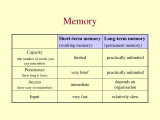
Types of Memories • Definitions • Write: store new information into memory • Read: transfer stored information out of memory • Random-Access Memory (RAM) • Can read and write • Read-Only-Memory (ROM) • Read only
Interesting Facts • Interesting fact of RAM: the time it takes to transfer information to or from any desired random location is always the same • A word =a group of bits • A group of 8 bits is called a byte.
Two Types of RAM • Static RAM (SRAM): Stored information remains valid as long as power is applied to the unit. • Dynamic RAM (DRAM): Stores binary information in the form of electric charges on capacitor provided inside the chip by MOS transistors.
74LS189 RAM 64 bits=16 4-bits words.
74LS189 RAM [A3,A2,A1,A0]=address inputs [D3,D2,D1,D0]=data inputs [S3,S2,S1,S0]=outputs ME,WE control the direction of transfer VCC=power GND=ground
Logic Diagram memory cell Each word is enabled by the 4-input AND
Logic Diagram memory cell Each word is enabled by the 4-input AND
Switching Time Waveforms 17 nS 23 nS A negative hold time means that the address/data can change before the rising edge of WE because the there is internal delay through the chip. -7 nS for address -14 nS for data
Write (ME=0, WE=0) D1 1 D2 1 D3 1 D4 [hi Z?] 1 1 0 0 0
READ (ME=0, WE=1) 0 1 1 Complement of data stored 0
HOLD (ME=1, WE=X) X 0 Hi-Z output 1
Memory Description in Verilog Need 6 bits address for 26=64 words. memory depth: 64 words word length 4-bits