Electron Beam Lithography
Electron Beam Lithography. William Whelan-Curtin. What is EBL for?. LPN. Nanopatterning High Precision Reliable Versatile . What is needed?. Very narrow, precisely controllable beam of Electrons Lots of money, a big complex machine, and a lot of expertise! . Outline.

Electron Beam Lithography
E N D
Presentation Transcript
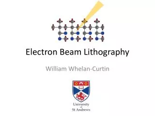
Electron Beam Lithography William Whelan-Curtin
What is EBL for? LPN • Nanopatterning • High Precision • Reliable • Versatile
What is needed? • Very narrow, precisely controllable beam of Electrons • Lots of money, a big complex machine, and a lot of expertise!
Outline • System description • Exposure • Examples
Electron “Pencil” • System Schematic
Electron source I Tungsten /Zirconium Oxide Tip -V • Tungsten wire (Thermionic) • 2300C • Energy Spread 2-3eV • Source size 25um • Thermal (Schottky) field emitter • 1800C • Energy Spread 0.9eV • Source size 20nm • Cold Field Emitter • 20C • Energy Spread 0.22eV • Source size 5nm Suppressor Higher Current density =>EBL Extractor (Anode) +V Unstable current 10-20% => SEM (High Vacuum ~10e-9mB)
Electron Lenses • Chromatic dispersion • Monochromatic beam • Aberrations • Use centre of lens F = q · (E+ v B) Electro-magnetic Electro-static
Electron Lenses • Magnetic versus Electrostatic Faster deflection Worse Aberrations EM lenses Simpler to implement
Beam Blanker • Turns the beam/off quickly • Control current for each pixel • High speed • Electrostatic Extractor +V +V
Column • Source • Apertures • Blanking • Collimation • Stigmation control • Deflectors • Focus • Final Lens (VISTEC VB6)
Types of Electron Beam Writer • SEM (Electron Beam “Reader”) • Generally magnetic lenses • Up to 30kV • Converted SEM (RAITH) • Addition of (fast) beam blanker • Pattern generator • Deflection needs time to stablise raster scan vector scan
Types of Electron Beam Writer • Purpose Built (LEICA/JEOL) • Better control, calibration • Up to 100kV • Higher speeds • Bigger writefields • Secondary deflection system Can also correct for aberrations in the primary lens
Types of Electron Beam Writer • Shaped Beam systems • Very complex optics • Higher current, lower resolution • Photomask making • (Not a research tool) GAUSSIAN
Patterning LPN • Electron sensitive polymer- the “paper”
Resist Overview “Positive” “Negative”
Electron-Solid Interactions Primary electrons • Forward scattering • Often • Small angles • High energy (~95% pass through the resist)
Electron-Solid Interactions Primary electrons • Back scattering • Rare • Large angles • Still High energy
Electron-Solid Interactions Primary electrons • Secondary electrons • Low energy (50eV) • Low penetrating power Responsible for exposure
H H H H C C C C H H H H H H H H H H H H H H C C C C C C C C C C C H H H H H O C O C O C C O n H H H H C O C O C O C O H H H H H H H H Electron Sensitive resist • Poly methyl methyl acrylate • Spin Coating • Long polymer chains H H C C H H H H H H C C C H H C C O O H H O O C C H H H H PMMA Substrate
H H C C C C H Electron Sensitive resist Secondary Electrons • Bonds broken (induced chain scission) • Dissolved by suitable chemical • Methyl Isobutyl ketone • Isopropanol:Water H H H H H H C C C C C C H H H H H H H H H H H H H H H H H H C C C C C C C C C C H H H H H H C C O O O C O C O C C O n H H H H H H O O C C C O C O C O C O H H H H H H H H H H H H PMMA Substrate
Contrast Curve Function of: Voltage Resist Thickness Substrate e.g. 170uAs/cm2 for 500nm thick PMMA on Silicon @ 30kV • Threshold electron density (lower≡faster exposure) • “Clearing Dose” or “Base Dose” • Slope -> Resolution Resist Thickness Dose (electrons/area)
Contrast Curve- Experimental • Determine for each new situation • Recheck regularly • Problem diagnosis Dose 50um
H H C C C C H Negative Resist Secondary Electrons • Microchem SU8 • Photo acid generator • Baking • Crosslinking • Acid Diffusion H H H H H H C C C C C C H H H H H H H H H H H H H H H H H C C C C C C C C C C H H H H H H C C O O O C O C O C C O n H H H H H H O O C C C O C O C O C O H H H H H H H H H H H H SU8 Substrate
Contrast Curve • Threshold electron density • Chemical amplification • Lower clearing dose Resist Thickness e.g. 1uAs/cm2 for 200nm thick SU8 on Silicon @ 30kV Dose (electrons/area)
Resolution J. Vac. Sci. Technol. B 12, 1305 (1975) • Most EBL systems -> 1nm spot sizes or less Vb 1nm Rt df df = effective beam diameter (nm) Rt = resist thickness (nm) Vb = acceleration voltage (kV)
Resolution EBL advice: Keep resist as thin as possible
EBL vs Focused Ion Beam etching • FIB • Energetic Gallium ions • Etching of the material • EBL • Modification • No removal of material Heavy ions Substrate
Electron-Solid Interactions Unintended Exposure! Primary electrons • Secondary electrons • Low energy (50eV) • Low penetrating power
Proximity Errors • Stray electrons • Bias t dose
Correction • Shape Correction • Difficult to generalise
Correction • Dose Modulation • Calculate the electron distribution • Reduce in certain areas 2 1
Electron Distribution Forward Scattering- α Back Scattering- β
Parameters • Depend on voltage/resist/substrate • Determine in each instance • Monte Carlo simulations • Experiment L. Stevens et al., Microelectronic Engineering 5, 141-150 (1986)
Correction Programs • Nanopecs, Proxecco • Pattern • Fracture • Calculate electron distributions • Alter pattern • Recalculate • Iterate until convergence is reached
Guidelines • PEC Computationally intensive • β<< pattern length scale << β (Homogenous background of scattered electrons) β =3.5um L=2um L=500nm L=50um
Laser Stage • Limited Deflection • Expose one “writefield” at a time • Laser interferometer controlled Stage movements • Calibrated • Sub 40nm accuracy • Pattern stitched together • Critical for Photonics
Writefield alignment θ ? 100um
Writefield alignment θ Xum
Liftoff • PMMA • Electron beam evaporation • Acetone
Liftoff • Metal thickness <1/3 of resist • Pure PMMA very effective at 30kV (or less)
Liftoff • Higher voltages • Better Resolution • Less forward scattering • Bilayer Resist Low molecular Weight PMMA
Etch back • Liftoff incomplete • Deposit metal , spin • Expose and develop • Dry etch Pmma Metal Substrate
Dry Etching • ZEON ZEP 520A • Xylene • Higher Sensitivity • Tougher
Dry Etching • ZEON ZEP 520A • High resolution, good etch resistance • Etch Quality crucial for many applications • Low selectivity etch • Thick Resist (400nm, @30kV)
Grayscale Lithography • SU8 Resist • Graded Dose
Grayscale Lithography • Dry etch into Silicon • Luneberg Lens Di Falco et al. Optics Express 19, pp. 5156 (2011)
The highest Resolution • Polymer resists • Resolution limited by chain length • Hydrogen silsesquioxane • Spin on Dielectric • Negative Resist Exposure/ Curing
HSQ 25nm period Grating • Highest resolution available • Good etch resistance 100kV Metal HSQ Substrate Diamond! <15nm dots Lister et al. Microelectronic Engineering 73--74, 319 (2004)
RAITH E-Line • Electron beam induced condensation • Gas fed into Chamber • 3D High Resolution Lithography Substrate

