Download
1 / 23
410 likes | 1.63k Views
Proximity Effect in Electron Beam Lithography. By Hussein Ayedh. Electron beam lithography (EBL). One of the most commonly used methods to pattern structures on a nanometer scale. EBL systems are a cornerstone of modern micro- and nanofabrication.

E N D
Proximity Effect in Electron Beam Lithography By Hussein Ayedh
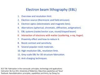
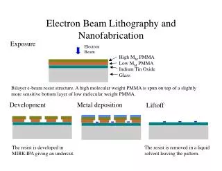
Electron beam lithography (EBL) • One of the most commonly used methods to pattern structures on a nanometer scale. • EBL systems are a cornerstone of modern micro- and nanofabrication. • Special electron beam sensitive resists have to be used for EBL. The most common one is polymethyl methacrylate (PMMA).
Electron beam lithography (EBL) • Two main electron sources: • Thermionic emission source Based on electron emission from a filament heated to a high T. • Field emission source Based on a field emission effect from a sharp W-tip.
Electron beam lithography (EBL) • Advantages • Extremely high resolution • Direct patterning on a substrate with high degree of automation (No mask required) • But: • Low throughput (Raster Scan) • Expensive (Vector Scan)
The proximity effect • A limiting factor of high resolution and contrast of EBL. • Depends on the pattern density and the substrate material, as well as parameters of the EBL exposure. • Acceleration voltage • Electron dose
The proximity effect • Source: backscattering and secondary electrons. • Secondary electrons are produced when an incident electron excites an electron in the sample and loses some of its energy in the process. The excited electron moves towards the surface.
The proximityeffect • The combined effect of forward scattering and backscattering broadens the electron beam. • The intensity distribution can be approximated by a sum of two Gaussian shapes. α : Forward scattering dispersion β : Backscattering dispersion η : Ratio of backscattered to forward scattered contribution
Approach • Study the proximity effect by exposing dot matrices on a resist and varying • Acceleration voltage • Electron dose • Density of dot matrices
Experiment • 200 nm of ZEP 520A7 resist on InP substrate. • Patterning in EBL. • Development in O-Xylene. • Evaporation of 20 nm of Au. • Lift-off in remover 1165. • SEM imaging.
Results at 10 kV Doses are in units of 0.01 pC
Doses are in units of 0.01 pC Results at 20 kV
Discussion • Acceleration voltage • Large voltage = better resolution • Electron dose • Large dose = larger dots and longer time • Density • Higher density = larger dots
Conclusion • Good resolution in this experiment was achieved by: • High acceleration voltage (20 kV) • Either high dose and low density or • Intermediate dose and intermediate density
Reduction of proximity effect • Proximity effect can be reduced by: • High electron energy (>100 keV). • Low electron energy (< 3 keV). • Thin resists. • Low Z material of substrate ( secondary electron yield is generally higher for high atomic number targets) • can be corrected by software.
Reduction of proximity effect Resist 10 keV Substrate 3 keV 100 keV
Reduction of proximity effect • High energy EBL: (>100 keV) • Dissipation of energy deep in substrate • Secondary electrons can not reach the surface to expose the resist. • Forward scattering in the resist is very small • Proximity effect is reduced! • But: expensive, big and complicated EBL system
Reduction of proximity effect • Low energy EBL: (1-3 keV) • Dissipation of electron energy in the resist only. • No generation of secondary electrons in the substrate! • Limitations: • Forward scattering is large -> low resolution. • E-beam size is big due to Column interaction between electrons. • Electron optics works poor at low energy. • Resist must be thin for complete exposure (e.g. 70 nm for 2 keV) difficult to use. • Hard to focus the e-beam, the beam is very sensitive to external fields
Reduction of proximity effect • Practical proximity effect correction: • Dose scaling: changes in exposure dose in parts of the structure. Dedicated software is used. • Shape correction: • (a) reduction of structure size and • (b) additional structures at underexposed areas • Dose scaling by software is the main method of proximity effect correction!
References [1] S.M.Sze ’’Semiconductor devices physics and technology ‘’2ND Edition ,willy ,2001. [2] S.A.Campbell ’’Fabrication Engineering at the Micro and Nanoscale‘’4th Edition ,Oxford ,2013. [3] G. May and S.M.Sze ’’Fundamentals of Semiconductor Fabrication‘’ ,willy ,2004. [4] Advanced Processing of Nanostructures Lecture note, FFFN01, Lund University.