Download
1 / 13
150 likes | 426 Views
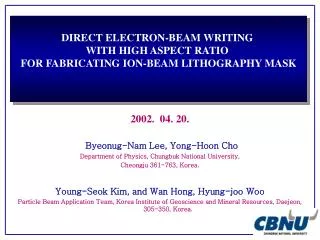
DIRECT ELECTRON-BEAM WRITING WITH HIGH ASPECT RATIO FOR FABRICATING ION-BEAM LITHOGRAPHY MASK. 2002. 04. 20. Byeonug-Nam Lee, Yong-Hoon Cho De partment of Physics, Chungbuk National University, Cheongju 361-763, Korea. Young-Seok Kim, and Wan Hong, Hyung-joo Woo

E N D
DIRECT ELECTRON-BEAM WRITING WITH HIGH ASPECT RATIO FOR FABRICATING ION-BEAM LITHOGRAPHY MASK 2002. 04. 20. Byeonug-Nam Lee, Yong-Hoon Cho Department of Physics, Chungbuk National University, Cheongju 361-763, Korea. Young-Seok Kim, and Wan Hong, Hyung-joo Woo Particle Beam Application Team, Korea Institute of Geoscience and Mineral Resources, Daejeon, 305-350, Korea.
h s Introduction • Lithography, it is that technology is able to transcribe narrow linewidth, exercises an effect on improvements in accumulation of DRAM and operation capacity of CPU. So, the main issue confronting the semiconductory industry is what the next generation lithography (NGL) should be. • Problems of optical lithography • The optical lithography can’t embody proven resolution below 0.1㎛. • (e.g., embodiment 0.13 ㎛ by ArF laser [193nm]) • Optical lithography has aspect ratio about with 1:1,so that it don’t suit MEMS's purpose.(MEMS needs high aspect ratio.) • aspect ratio: h / s • Masked Ion Beam Lithography (MIBL) is one of the most promising candidates. MIBL is a technology to produce advanced, very large scale integrated (VSLI) and nanometer-scale circuits. The strengths of MIBL include proven resolution below 0.04㎛, wide exposure latitude, large depth of field, high throughput, and the possibility of avoiding substrate damage.
Drawing tool AutoCAD-polyline Writing tool Home made writing program COMPUTER COMPUTER COMPUTER COMPUTER COMPUTER COMPUTER dxf.file COMPUTER COMPUTER COMPUTER COMPUTER DA DA DA DA (digital (digital - - to to - - analog) analog) (digital - to - analog) (digital - to - analog) converter (5MHz) converter converter converter E E SEM SEM SEM SEM (Scanning Electron Microscopy) (Scanning Electron Microscopy) (Scanning Electron Microscopy) (Scanning Electron Microscopy) E-beam writing system • Output voltage control • Control signal=output voltage(V) • 32768 10 (= Max V) • * Analog out put: 2 • * Analog range: -10~ +10v • Output voltage: divide into 65536 (16 bit)
PMMA 0.4 ㎛ Au 0.03 ㎛ Ion beam Ti 0.003 ㎛ Si3 N4 4㎛ Si Si(B) ,Si3N4 Ti Au Si Structure of blank & Final Ion-beam Mask Blank Mask Final Ion-beam Mask f
65536 mask Faraday cup Standard sample 65536 Summaryof sample stage & e-beam lith. • Acc. voltage: 40 KeV • Writing시 Beam current :10 ~ 20 Pa • Writing시 magnification : × 1000 • Focusing magnification on Standard sample : × 300,000 • A screen of SEM is divided into a lattice of 65536 × 65536. • The position of electron beam spot is lineally changed by run voltage • Every lattice has voltage rectangular coordinates ; (Vx,Vy)
a) b) 50nm 16nm 50nm Designed pattern Pattern designs • The Pattern designs is using AutoCAD. • A space between two points is 1㎛ on Auto CAD coordinates.
Aspect Ratio & Line width • E-Beam Writing • Focusing • dosage • Beam energy • Develop • - Developer • - Temperature • - Time • Blank Mask • - Resist thickness • - Resist uniformity Primary factorof aspect ratio & linewidth
0.08㎛ 디자인 선 폭의 현상조건 실험 * 빨간 글씨: 최적 조건
0.08 ㎛디자인 선 폭 최적화 조건 * 빨간 글씨: 최적 조건
0.08 0.08 0.08 ㎛ 디자인 ㎛디자인 ㎛디자인 0.08 0.08 0.08 ㎛ 디자인 ㎛디자인 ㎛디자인 350 350 350 μ μ μ c c c / / / ㎛ ㎛ ㎛ 2 2 2 350 350 350 μ μ μ c c c / / / ㎛ ㎛ ㎛ 2 2 2 0.135(㎛) KIGAM 20KV KIGAM 20KV KIGAM 20KV KIGAM 20KV KIGAM 20KV KIGAM 20KV × × × 35,000 8mm 35,000 8mm 35,000 8mm × × × 35,000 8mm 35,000 8mm 35,000 8mm 0.08 ㎛디자인 선 폭 최적화 조건 * 빨간 글씨: 최적 조건
0.05 ㎛디자인 선 폭 최적화 조건 * 빨간 글씨: 최적 조건
Summary • Masked Ion Beam Lithography (MIBL) is one of the most promising candidates차세대 노광 기술인 이온 빔 노광 기술 용 0.1 mm 이하의 선 폭에 종횡비가 1:7인 마스크 개발 목표로 실험을 수행하였다. • A multiple-pass writing method has been implemented, which has significantly improved image placement of final ion beam masks. This method was optimized for image-size and defect performance on the e-beam lithography system. Image placement of 60nm was achieved. we could obtain an e-beam writing pattern with a line-width of ~ 80 nm and an aspect ratio of 1:5~. • 실험결과는 Proximity Control 한 결과와 하지 않은 결과로 나누어 볼 수 있는데, Proximity Control 한 결과 디자인 선 폭과 유사하게 현상되었다.실험은 0.086 선 폭에 종횡 비 1:4.65인 패턴을 형성하였다. • 패턴 형성은 Proximity Control 한 결과가 계선 되었다.

![Electron [and ion] beam studies of magnetic nanostructures](https://cdn2.slideserve.com/4692681/slide1-dt.jpg)