Download
1 / 25
280 likes | 357 Views
Explore e-beam lithography basics, pattern handling techniques, and hardware concepts in this comprehensive guide. Learn about key concepts like dose, pattern generation, and pattern stepping to optimize your e-beam writing processes efficiently.

E N D
Basics E-beam lithography Introduction of concepts Pattern handling Hardware issues Miscellaneous
Main issuesIntroduction of concepts Resist • Dose [µC/cm²] Pattern • From design to beam stepping Electron Beam Pattern Generator • Holder/substrate • Positioning • Beam • Exposure
Electron Beam Pattern GeneratorIntroduction of concepts • Source Field Emission Gun • Beam column spot, scanning beam • Stage/holder substrate, stepping, controls
Substrate holderIntroduction of concepts • Beam current measurement • Calibrations (spot size, focus) • Orientation reference (x,y)
E-beam definitionsIntroduction of concepts • Dose (material, kV) µC/cm² • Acceleration voltage kV (20kV, 50kV, 100kV) • Spot size dspot 3 … 175 nm • Beam current Ispot (~dspot²) 300 pA … 317 nA • Beam step size BSS • Resolution Res • Beam step frequency BSF 500 Hz … 100MHz
From pattern to e-beam writing processpattern handling Hardware • Stage movement • Beam deflection Fracturing • Main field (scanfield, block) • Trapezium
Large structurespattern handling • pattern divided into main fields • substrate move for each next main field • main field exposure by beam deflection each main field: • beam @ center main field • height compensation • deflection calibrated to stage movement Writing order of main fields
Trapeziumpattern handling T = pixel exposure time BSF (MHz) = 1/T(µs) Ispot(nA) 1 = 0.1 * ------------------------------- ~ ---------- Q(µC/cm²)*BSS²(µm²) dspot²
Trapezium-wise beam stepping in main fieldpattern handling Each (xi,yi) is the start of a new trapezium
EBPG CHARACTERISTICSpattern handling • Trapezium resolution 0.08 nm ……… 0.5 nm • Main field resolution 0.16 nm ……… 1.0 nm • Main field deflection º max field size = 1048576*mainresolution (20bits) º size range: 167.8 …1048.576 µm @ 100kV • Trapezium deflection º BSF: 500 Hz – 100 MHz º BSS = 1,2,3,4,5,…,16383 * trapezium resolution º max field size = 16384 * trapezium resolution (14bits) º size range: 1.31 … 4.525 µm @ 100kV
Filling the pattern with spotspattern handling • e-beam is stepped • filling areas use dspot=1.2–1.5*BSS • lines use minimal 4-5 spots in linewidth • narrowest lines º take smallest spot º define linewidth of 1 BSS (often 1.25nm)
Intermezzo: dose considerationsprimary and secondary contributions • primary dose º lateral range: spot diameter + little effect from forward scattering in resist º gaussian distribution º partial overlap of adjacent spots • secondary electrons lateral range: 5 nm around primary electron path • backscattered electrons (proximity) º lateral range: many µm º on Si, at 100 kV typically 50 µm º gaussian distribution … different dose settings for plane, line and spot
Intermezzo: dose considerationsprimary and secondary contributions
JOB TIMEpattern handling • beam-on time Q(µC/cm²)*A(mm²) 1 1 T(s) = 10* --------------------------- ~ --------- ~ --------- Ispot(nA) BSS² dspot² • to minimize beam-on º split coarse and fine pattern layers, but keep small (e.g. 1 µm) overlap º calibration per layer takes 3 to 5 minutes • overheads º main settling 50µs/trapezium º stage movements º big pattern files (max 1GB!)
Software and computer overviewpattern handling Software • DesignAutocad/DesignCAD/LDM-file/L-Edit/Other • Output formats DXF/ GDSII/ CIF/ TXL/ other formats • Conversion LayoutBeamer gpf pattern data • Gpf pattern data exposure EBPG Cview inspection Computer Layout Beamer PG5000+ USER ---------------------- pegasus ---------------------- EPIC-ALFA (design) (job) pegasus.kavli.tudelft.nl epic-alfa.kavli.tudelft.nl cad/&KN-lab pg/pg5000@Delft or PG5200 EPIC-BETA epic-beta.kavli.tudelft.nl pg/pg5200@Delft
Around the stagehardware issues • BSED: Back Scattered Electron Detector • locating marker • spot optimization and focussing • Laser: height measure-ment beam focus on substrate
Substrate holderhardware issues • Cup: current measurement, x-y reference • Markers: spot characteristics
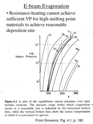
Beam current measurementhardware issues Faraday cup
Calibration markershardware issues • spot optimisation (focussing) • spot size measurement • ‘zero’ height reference • reference in (x,y) position • marker search
Spot size measurementhardware issues dmeas² = dspot² + dedge² dedge = 20nm for very good marker but often > 30nm; depends on marker edge itself and possible contamination dmeas² = a.Ispot + b (small spots)
Spot size adjustmenthardware issues FEG: high brightness electron source BSF too high need for defocus • discrete steps of 20nm/bit in FL@400 µm aperture • adds quadratically to initial spot dadjust² = dmeas² + ddefocus² • unround spot if a few bits • real big spots: 4/3*measured size • defocus to dmeas or adjust by [+ -]<bits>
Height adjustmenthardware issues Beware: • Transparent substrate • Reflectivity topology • Flatness: 1µm/mm height error ~ 1.5µm broadening of the beam with ~ 7.5nm (at 400µm aperture) Calibration marker at ‘zero’ height Adjustment range; ± 100 µm
Height levelhardware issues final lens image of spot on substrate • Substrate NOT at constant height should be < 1µm/mm • Height compensation during exposure: • spot size –FF • scaling • rotation • Final aperture MUST be well aligned
E-beam threatsmiscellaneous • Charging • e-drain required conductive layer* • Contamination • work clean! • handle holders carefully and with gloves • Vibrations • turbo: around 800Hz writing strategy!* • don’t be around during writing • Thermal stability • Keep door closed * In more detail in Advanced E-beam Litho
Limitationsmiscellaneous • Resist • shot noise: N ± √N • swelling • secondary electrons: 8nm extra • Position accuracy • laser interferometer: 0.6nm • marker location: 30nm • drift (0.1 µm/hr possible) • main field overlay • stitching: 60nm