Download
1 / 25
250 likes | 547 Views
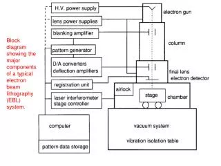
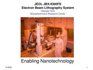
JEOL JBX-9300FS Electron Beam Lithography System Georgia Tech Microelectronics Research Center. Enabling Nanotechnology. Nanoimprint Embossing Stamps Researcher: Andrew Ballinger*, Devin Brown** *University of North Texas, **Georgia Tech Microelectronics Research Center. NIL. Plasma Etch.

E N D
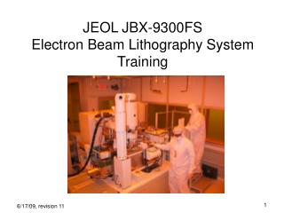
JEOL JBX-9300FS Electron Beam Lithography System Georgia Tech Microelectronics Research Center Enabling Nanotechnology
Nanoimprint Embossing Stamps Researcher: Andrew Ballinger*, Devin Brown** *University of North Texas, **Georgia TechMicroelectronics Research Center NIL Plasma Etch EBL HSQ resist 20 um stamp resist trim Silicon substrate spin coat 3.5nm gap PMMA resist 7nm oxide e- e- e- e- e- Silicon substrate 10 MINUTES!! / REUSABLE imprint silicon etch 10 HOURS!! exposure resist strip resist strip develop 80nm line 70nm space 30nm diameter 11nm 150nm line 80nm line
adhesive protein protein resistant group Au PR Si Nanopatterned Protein Arrays Graduate Student: Sean Coyer, PI: Andres Garcia Biomedical Engineering, Georgia Tech pattern protein EBL + metal lift-off 500 nm 250 nm 5 mm E-beam Lithography is used to produce patterned arrays presenting adhesive protein islands within non-fouling background to analyze cell adhesion. 100 mm cells
Nanoscale Resonator Researcher: Michael Kranz*, Mark Allen** *Stanley Associates, **Georgia TechElectrical Engineering 20 um 3.5nm gap An array of these nanoscale resonators form a high-speed parallel-processing spectrum analyzer for signals in the 100's to 1000's of MHz. A two-step hybrid lithographic approach allowed the large features of the device, including anchors, RF waveguides, and electrodes to be patterned using traditional optical lithography after the micron, submicron, and nanoscale features were patterned using Georgia Tech's JEOL EBL system. The device was formed in a thin silicon film sputtered on top of a thin silicon dioxide film that served as a release layer during a standard HF oxide etch. Patterning was accomplished through first exposing a PMMA electron beam resist and subsequently transferring that pattern to a thin chrome layer used as a mask for transferring the pattern to the device silicon.
Chemically Amplified Resist for Nanoscale Patterns Researcher: Cheng-Tsung Lee, Cliff Henderson Georgia TechChemical and Biological Engineering Patterns on nitride membrane 20 um 3.5nm gap 30nm line/space Film thickness: 75nm Shot pitch: 10nm Current: 2nA; Dose: 120 uC/cm2 30 nm half pitch pattern on novel EUV resist • High acceleration voltage (100kV) electron-beam lithography on ultra-thin silicon nitride substrate provide the excellent tool in determining the intrinsic resolution of the novel chemically amplified resists. • Novel EUV resist shows the inherent resolution in patterning 30 nm half pitch line/sapce array with low CD variation and LER.
CPP-GMR spin valves Researcher: Cristian Papusoi, Su Gupta University of Alabama at Tuscaloosa 20 um 3.5nm gap Top lead Bottom lead Contact hole (100 nm diameter) SV pillar (stack) 9 mm diameter Giant MagnetoResistive (GMR) devices are potential candidates for magnetic read heads. The Current Perpendicular to the Plane (CPP) geometry, when the current is flowing perpendicular to the film plane, is expected to deliver the maximum sensitivity (GMR ratio).
Advanced Dielectrics and Lithography for Interconnects Roey Shaviv, Novellus Devin Brown, Georgia Tech 40nm ZEP520A resist Dielectric test structure SiO2 Silicon substrate Research is being done on advanced dielectric materials for creating 40 nm and below interconnect lines to meet ITRS objectives for the 32 nm technology node.
SOI Photonic Crystals Researcher: John Blair*, Stephen Ralph** *Georgia Tech Material Science, **Electrical Engineering Resonant cavity photonic crystal pattern that resonate at 1.55um wavelength, infra-red.
Optical Diffractive Element Researcher: Anonymous External Customer, Devin Brown Georgia Tech 70nm diameter holes in 80nm Aluminum on quartz substrate using lift-off technique.
Nanometer Gaps Researcher: Raghunath Murali, Farhana Zaman Georgia TechMicroelectronics Research Center • Si substrate, Resist : 47 nm thick PMMA • E-beam lithography with 2 nA current, 100 kV acc. voltage • Metal liftoff process with 5 nm Cr adhesion layer and 10 nm Au 20 um 3.5nm gap 13.2 nm gap
Nanoresonator Researcher: John Perng, Farrokh Ayazi Georgia TechElectrical Engineering 37nm-wide electrode gap capacitive block resonator • High frequency MEMS resonator are used in many different applications, such as RF oscillator, on-chip frequency reference, biosensor, etc. • Capacitive-based resonator requires small electrode gap to increase signal to noise ratio and to lower motional impedance • The goal of this project is to characterize the limit of nano trench etching in Si (10nm-wide, max depth?) and produce working device with sub-100nm gap
Negative Index Photonic Crystal Superprisms Researcher: Babak Momeni, Ali Adibi Georgia TechElectrical Engineering • beams of different wavelengths propagate in different directions inside the PC (superprism effect) • negative refraction of the separated channels results in their separation from undesired light (noise, scattering, unwanted polarization, and out-of-range wavelengths) in the incident beam, thus reducing the overall noise level • four channels are separated in this device with a wavelength spacing of 8nm
Cancer Diagnosis Bio-Assay Nano Cantilever Array Researcher: Kevin Klein, Jiantao Zheng, Suresh Sitaraman Georgia TechMechanical Engineering 20nm cantilevers • nanocantilevers can be individually coated with specific reagents to detect and measure the presence of particular antigens and/or complementary DNA sequences with a smaller sample size and at much earlier stages of disease progression compared to current medical diagnostic technologies • high-throughput detection of proteins, DNA, and RNA for a broad range of applications ranging from disease diagnosis to biological weapons detection
resist pattern PECVD SiO2 Si-wafer Interlevel Spin-coated S/P PECVD SiO2 CMP stop layer Spin-coated S/P resist pattern PECVD SiO2 PECVD SiO2 Si-wafer CMP CMP stop layer Si-wafer Spin-coated S/P Spin-coated S/P PECVD SiO2 PECVD SiO2 Si-wafer resist pattern CMP stop layer Si-wafer Spin-coated S/P Si-wafer metal barrier layer PECVD SiO2 Spin-coated S/P PECVD SiO2 Cu layer metal barrier layer Si-wafer CMP stop layer Spin-coated S/P Spin-coated S/P PECVD SiO2 PECVD SiO2 Si-wafer Si-wafer Si-wafer Ultra Low K Damascene Process Extended Air Gaps Researcher: Seongho Park, Paul Kohl Georgia TechChemical & Biomolecular Engineering Deposition of the interlevel dielectric RIE etching of SiO2, PR is etch mask. Wet etching of Cu Decomposition of S/P Interlevel resist stripping and spin coating of S/P Intralevel Cu PECVD SiO2 Si-wafer deposition of CMP stop layer and resist patterning (e-beam lithography) Electroplating of Cu or CVD Cu RIE etching of CMP stop layer Deposition of metal barrier layer Deposition of Cu seed layer resist pattern CMP stop layer Spin-coated S/P PECVD SiO2 Si-wafer Stripping e-beam resist and RIE for S/P
Advanced Copper Interconnection and Low-k Dielectric Researcher: *Dean Denning, **Devin Brown *SEMATECH, **Georgia Tech 30 nm lines Research on advanced copper interconnects and low-k dielectric material is being carried out at Georgia Tech, with interconnect line widths down to 30 nm to address needs and challenges presented by the International Technology Roadmap for Semiconductors (ITRS). SEMATECH members include Infineon, AMD, Intel, HP, IBM, Samsung, TI and Freescale.
Carbon Nanotube Pattern Control Researcher: Devin Brown, Azad Naeemi Georgia Tech Microelectronics Research Center < 20nm pattern alignment ! Research is being conducted to study the effects of electric field during carbon nanotube growth. The image above shows 100nm diameter Iron catalyst islands aligned to less than 20nm on top of 100nm Molybdenum electrode lines.
LASER Detector Raman “Fingerprint” Single Molecule Detection Graduate Student: Chris Tabor, PI: Mostafa A. El-Sayed School of Chemistry, Georgia Tech 7nm gap Hazardous substances such as Cyanide and Anthrax could be confidently and efficiently detected below the infectious concentration. As the particle separation increases the detection limit increases exponentially. It is thus imperative that the particle gaps be on the order of a few nanometers and is why EBL is so important to the fabrication technique.
Graphite Nanotransistor Graduate Student: Zhiming Song, PI: Walt De Heer School of Physics, Georgia Tech 20nm Nanowire is formed in a thin graphite layer to produce a transistor similar to carbon nanotube.
Silicon Photonic Crystals Graduate Student: Tsuyoshi Yamashita, PI: Chris Summers Materials Science & Engineering, Georgia Tech Photonic crystal devices provide researchers with numerous properties unavailable in conventional optical materials such as the negative index of refraction effect.
Narrow Isolated Line Resolution Devin K. Brown, Raghunath Murali Microelectronics Research Center, Georgia Tech Best result to date (2/16/05): 6.5nm line Isolated line in negative HSQ e-beam resist.
Narrow Dense Lines Resolution Raghunath Murali, Devin K. Brown Microelectronics Research Center, Georgia Tech Dense lines in positive ZEP520 e-beam resist.
SiO2 Au Au 40 nm 300 nm 30 nm SiO2 Electroluminescence of Gold Nanoparticles Graduate Student: Wonsang Au, PI: Robert M. Dickson School of Chemistry and Biochemistry, Georgia Tech Exhibiting characteristic single-molecule behavior, these individual room-temperature molecules exhibit extreme electroluminescence enhancements (>104 vs. bulk and dc excitation on a per molecule basis) when excited with specific ac frequencies.
Georgia Research Alliance Graduate Student: George P. Burdell School of Engineering, Georgia Tech 13nm 13nm line width lettering in negative HSQ EBL resist.
26nm feature Georgia Tech Buzz Mascot Graduate Student: George P. Burdell School of Engineering, Georgia Tech 26nm features in positive ZEP520 EBL resist.
JEOL JBX-9300FS Electron Beam Lithography System http://nanolithography.gatech.edu