Download
1 / 1
10 likes | 93 Views
Explore angular dependency of ion flux & power on Cu(111) etching process. Analyze energy yield & ionization fraction impact with relevant simulations and findings from scholarly research.

E N D
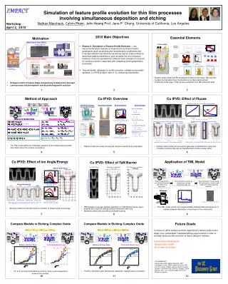
Angular dependency Total Ion Flux (Ar+ and Cu+) vs. Power Total Cu flux and ionization fraction vs. Power Ar+ on Cu(111) M M M Angular dependent etching Cl Cl Cl B B B O O O Ion Scattering Neutral Adsorption + + + + + + + + + Vyas, V., Kushner, M. JVST A 24(5) 2006 + + + + + + + + + Sample simulations with flux ratios from above Ion Adsorption Cu+ on Cu(111) Energy dependency + Overhang from sputter Physical Sputtering Ar+ on Cu (111) 45° off normal scattering Liu, X.-Y. et al. Thin Film Solids 422, 2002 Ion Etching Ion Induced Production 21% Cu+, 16% Cu 63% Ar, Eion = 25, sE = 10 75% Cu+, 20% Cu, 5% Ar+ Eion = 50, sE = 10 11% Cu+, 33% Cu 56% Ar , Eion = 25, sE = 10 7% Cu+, 42% Cu 51% Ar , Eion = 25, sE = 10 Henrik Schumacher, CMOS Chip Structure. www.wikimedia.org + 85% Cu+, 20% Cu, 5% Ar+, Eion = 50, sE = 10 Spontaneous Removal by incoming C flux Angular Dependencies of Ion etch yieldKress, J. D. et al. JVST A 17(5), 1999 E=15 eV, sE = 10 25 eV, sE = 10 35 eV, sE = 10 45 eV, sE = 10 q 10 kW Power 30 kW Power 50 kW Power Increasing Energy (Flux ratio constant 75% Cu+, 20% Cu, 5% Ar+ High Neutral to Ion ratio results in very low bottom deposition Cu+ Sputtering of Cu (111) Angular Dependence Coronell et al. APL 73(26), 1998 Surface normal is calculated using polynomial fitting High k Poly Porous Low k SiO2 SiO2 Si NiSi, NiSi(Pt) After Poly Etch Poly High k Via etch: top view Metal SiO2 Gas flow rate SiO2 Si High k After High k Etch Profile evolution Simulations with higher ionization ratios Top View Higher ionization ratio and energy yields higher bottom coverage and faceting Simulation of feature profile evolution for thin film processes involving simultaneous deposition and etching Nathan Marchack, Calvin Pham, John Hoang Prof. Jane P. Chang, University of California, Los Angeles 2010 Main Objectives Essential Elements Motivation Back End of Line (BEOL) Cu ionized PVD • Plasma 3. Simulation of Feature Profile Evolution – Use experimental beam systems to measure the pertinent kinetics parameters (such as sticking and recombination coefficients and formulate reaction mechanisms) as well as reactor scale models (to determine plasma parameters, such as wafer flux and ionization fractions) to be incorporated into a Monte Carlo simulator to account for surface evolution, especially with competing etching/deposition processes • Expand kinetic database for profile evolution; validate using model systems: Cu IPVD & High-k etch in Cl2 containing chemistries Singer, Peter, Semi. Int. 2008 Front end of Line (FEOL) Current Generation MOSFET Structure Selective High k Gate Etch TEM Micrography of Current Generation High k Devices Adapted from http://finepolymers.com/feol-cleans • Reactor scale model and PIC/analytical model provide fluxes, IED and IAD • Surface normal determines the direction of surface advancement • Translated mixed layer (TML) kinetics extracted from MD and beam data Braun, A.E. Semi. Int. (2000) Auth, C. et al. Intel Tech. Journal (2008) • Stringent control of feature shape and geometry as dimensions decrease • Lower process and development cost by predicting profile evolution Method of Approach Cu IPVD: Overview Cu IPVD: Effect of Fluxes Reactor scale flux ratios with varying power SEM Courtesy of Novellus Systems HCM IPVD Reactor Physics Models Kinetic Models Simulation Domain Large bottom to top coverage ratio indicates high Cu ionization fraction Singer, Peter. Semiconductor International 2002 Vyas, V., Kushner, M. JVST A 24(5) 2006 • The TML model allows for individual reactions to be modeled and provides information about the surface composition. • Reactor scale model can be used to generate normalized flux ratios and ionization fractions that can be implemented to feature scale model • Robust model can easily incorporate complex kinetics and composition Cu IPVD: Effect of Ion Angle/Energy Application of TML Model Cu IPVD: Effect of TaN Barrier Sticking on sidewalls No Sticking on sidewalls Cu IPVD Data SEM Courtesy of Novellus Systems Eion Adsorption Flux Removal Flux Γion Γneutral Movement Flux Final verification involves using TML parameters in feature scale model and comparing profile evolution. Perform experiments with selected materials and chemistry to obtain data. Test parameter accuracy by comparing to surface composition data, etc. Faceting observed due to angle dependant etching Increasing RF Power SEM Courtesy of Novellus Systems Hoang et al. JVST B 26(8) 2008 • The TML model is built from experimentally obtained data and allows for a realistic physical description of a process to be constructed. • SEM images show low sidewall deposition on TaN diffusion barrier layer, possibly as a result of lacking surface interactions with ions • Modeled profiles with and without sidewall sticking • Sticking coefficient and etch yield is a function of impact angle and energy Compare Models in Etching Complex Oxide Compare Models in Etching Complex Oxide Future Goals • Continue to refine surface evolution algorithms in feature scale model • Apply more complicated Translated Mixing Layer kinetics in order to simulate feature profile evolution of high-k dielectric material • Special Acknowledgements • Herbert Sawin at MIT • Ron Kinder at Novellus Goal 1 Goal 2 Eion Eion Adsorption Flux Removal Flux Adsorption Flux Removal Flux Γion Γion Γneutral Γneutral Movement Flux Movement Flux Balance Surface Sites Translating Mixed Layer Balance Surface Sites Translating Mixed Layer Funded by • For BCl3 chemistry, both etching and deposition regimes can be modeled. • For a Cl2 process dominated by etching, there is good agreement between the models.