Download
1 / 6
70 likes | 212 Views
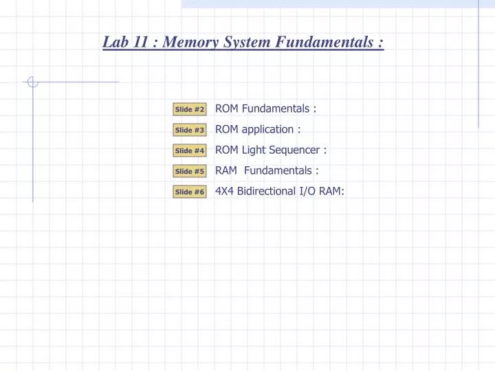
Lab 11 : Memory System Fundamentals :. ROM Fundamentals :. Slide #2. ROM application :. Slide #3. ROM Light Sequencer :. Slide #4. RAM Fundamentals :. Slide #5. 4X4 Bidirectional I/O RAM:. Slide #6. Burnt fuse = Transistor Cut-off. Fuse intact = Transistor Saturation.

E N D
Lab 11 : Memory System Fundamentals : ROM Fundamentals : Slide #2 ROM application : Slide #3 ROM Light Sequencer : Slide #4 RAM Fundamentals : Slide #5 4X4 Bidirectional I/O RAM: Slide #6
Burnt fuse = Transistor Cut-off. Fuse intact = Transistor Saturation Tri-State Bufferwith active lowenable. Thus HiZ out! 0 0 0 1 1 0 0 1 1 0 Data Bus = Cell Q0 Data Bus = Cell Q1 Data Bus = Cell Q2 1 0 1 1 =E 0 1 0 1 Data Bus = Cell Q3 Lab 11: ROM Fundamentals : The internal construction of a 4 Bit ROM can be used to introduce ROM fundamental concepts. The equation used to describe the storage capacity of the ROM is 4X1 ( four 1 bit memory cells). Each cell is a transistor with a programmable fuse. To store a 1 leave the fuse intact. To store 0burn out the fuse. As you can see the Address Bus controls which memory cell sends its data to the Data Bus. Each memory cell has its own address just like each house on a street is identified with an address. The house address identifies the occupants (data). The memory address identifies the binary data in a memory cell. The Control Bus can shut down the Data Bus. The Data Bus can be put into HiZ if the CS=1. The content of the memory cell is accessed via the Data Bus pin. The CS (Chip Select) input makes up the Control Bus. For CS=0 the chip is selected and memory can be accessed. For CS=1 the memory cannot be accessed and the Data Bus = HiZ. The CS pin will be connected to GND. This will enable the decoder and make one of the decoder outputs active (logic 0). The Address Bus pins determine which decoder output that gets asserted. IF address = 0,0 then output 0 of the decoder will be asserted. The top tri-state buffer is asserted. The data bus will come out of HiZ and output the contents of the Q0 memory cell. Address Bus Here is what happens if address = 0,1 Data Bus Here is what happens if address = 1,0 Here is what happens if address = 1,1 Control Bus CS is the Enable input of 1 of 4 decoder. CS= 1 disables decoder. All outputs (O0, O1, O2, O3) =1. Slide #2 Logic 1 at the enable input of the tri-state buffer will make the Data BusHiZ (open circuit/no signal)
1 0 0 1 0 1 0 1 1 0 0 Yes De-scramble Yes de-scramble! Do not de-scramble 1 0 0 1 1 0 1 0 1 Do not de-scramble Lab 11 : ROM Pay TV System Application : ROM memory IC’s must first be programmed before they can be used in a computer system. To illustrate this, let’s assume the 4 bit ROM is used in a 1st generation PAY TVde-scrambler system. Many years ago a PAY TV de-scrambler system was nothing more than a computer that read (accessed) the content of a ROM to see what channels would be de-scrambled. Let’s assume the de-scrambler allows a customer to choose among 4 PAY TV channels. Let’s assume the customer requests a de-scrambler that can de-scramble only the first 2 channels. The cable company would receive a call from the customer and would program the ROM. A blank ROM would be inserted into a programming station and the bottom 2 fuses would be burnt. The ROM would be inserted into the PAY TV de-scrambler computer system and given to the customer. The customer would attach the system to their TV. On power up the computer would need to cycle the address bus inputs while reading the data bus to see which channels need de-scrambling. A ROM must be programmed before it can be used in a system. The contents of ROM are read (accessed) sequentially (one cell after the other) by the computer system. Slide #3
Add. Bus Add. Bus Data Bus Data Bus 3 2 1 0 3 2 1 0 3 2 1 0 3 2 1 0 7 6 5 4 7 6 5 4 0 0 0 0 0 0 0 0 0 0 0 1 0 0 0 1 0 0 1 1 0 0 1 0 0 1 0 0 1 0 0 0 0 1 1 0 0 0 0 1 0 0 0 0 0 0 0 0 0 0 0 0 0 0 0 0 0 0 0 0 0 0 0 0 0 0 0 1 0 0 0 0 0 0 0 0 0 0 0 1 0 0 0 0 0 0 1 0 0 0 0 0 0 0 0 0 0 0 0 0 0 0 0 0 0 0 0 0 0 0 0 0 0 0 0 0 0 0 0 0 0 0 0 0 0 0 0 0 0 0 0 0 1 0 0 0 0 1 0 0 0 0 0 0 0 0 0 0 0 0 0 0 0 0 0 0 0 0 0 0 0 0 0 0 0 1 1 0 0 0 0 0 0 0 0 0 0 0 0 0 0 0 0 0 0 0 0 0 0 0 0 0 0 0 0 0 0 0 0 0 1 1 0 0 0 0 0 0 0 0 0 0 0 0 0 0 0 0 0 1 0 0 1 1 0 0 0 0 0 0 0 1 0 0 1 0 0 1 0 0 1 0 0 0 0 0 0 0 1 0 0 0 1 0 0 0 0 1 0 0 0 0 1 0 0 0 0 1 0 0 0 0 16X8 ROM 0 0 1 0 0 0 1 0 0 0 1 1 0 0 1 1 D0 0 1 0 0 0 1 0 0 D1 0 1 0 1 0 1 0 1 0 1 1 0 0 1 1 0 Q0 A0 D2 0 1 1 1 0 1 1 1 Q1 A1 D3 1 0 0 0 1 0 0 0 >clk 1 0 0 1 1 0 0 1 Q2 A2 D4 1 0 1 0 1 0 1 0 Q3 A3 D5 1 0 1 1 1 0 1 1 1 1 0 0 1 1 0 0 D6 1 1 0 1 1 1 0 1 CS D7 1 1 1 0 1 1 1 0 1 1 1 1 1 1 1 1 Lab 11 : 16X8 ROM Light Sequencer: We will use a 16X8 ROM to create a light sequencing system. This application will also introduce the concept of a Memory Map Diagram. A 16X8 ROM can store 16 different 8 bit data codes. To store 16 codes the ROM requires 4 address inputs (24=16). The data stored in the ROM will be read (transferred) to 8 LED’s. Note: Logic 1 = LED on … Logic 0 = LED off. The address inputs will be cycled by a mod 16 counter. A Memory Map Diagram is a table that shows the content of a programmed ROM. A blank ROM has all data at 0. Here is the Memory Map Diagram of a blankROM. The user of a ROM decides what data codes are needed for the application and generates a Memory Map Diagram. The diagram is used to program the IC. Here is the diagram for the Light Sequencer. Attach a 1 PPS clock to the input of the counter and this is what you will see on the LED’s. Use the backspace key to replay the animation. To change the light sequence pattern all you need to do is erase the ROM, create a new Memory Map Diagram, re-program the ROM and re-insert it into the system. This type of change is much simpler than a complete re-design of an entire logic system. Slide #4
0 1 1 0 0 0 0 0 0 0 0 0 0 0 0 0 0 0 0 0 0 0 0 0 0 0 0 0 0 0 0 0 0 0 0 0 0 0 1 0 0 1 0 0 0 0 1 0 0 1 1 1 0 0 0 0 0 0 0 0 0 0 1 0 1 0 0 1 1 0 0 1 Lab 11 : RAM Fundamentals: A 64X4 SRAM is a StaticRAM. It has 6 address pins (26 =64). Static implies that the memory cells, in each 4 bit register, are flip flops. It has bidirectional I/O pins. An SRAM is used to write data and to later read it back. Let’s assume the SRAM has all 64 data codes are 0,0,0,0. Write Operation Example:Write the number 9 into register 2.Step 1: Apply signals to the Address Bus. Register 2 = Address 2. Step 2: Apply signals to the Data Bus. Data =9 =1001. Step 3: Apply signals to the Control Bus. R/W=0 to write … CS=0 to enable IC.This will enable the Input Buffers. Output Buffers stay in HiZ (no contention). In the write mode all pins on the SRAM must be driven. All pins are inputs. Read Operation Example:Read the number 9 from register 2.Step 1: Apply signals to the Address Bus. Register 2 = Address 2. Step 2: Make sure you are no longer driving the Data Bus pins. Reading means the data bus will output the number 9. Connect LED’s to data bus if you would like to display the number. Step 3: Apply signals to the Control Bus. R/W=1 to read … CS=0 to enable IC.This will enable the Output Buffers. Input Buffers are in HiZ. In the read mode the Address and Control Bus pins must be driven. The Data Bus pins are outputs and must NOT be driven. Driving the Data Bus pins could result in damage to the IC. Slide #5
When “OE” = 0 the “Output Buffers” are NOT enabled and can no longer be controlled by “WE”. They remain continuously in “HiZ” regardless of the condition at “WE”. “OE” is called “output enable”. “OE” can be used to enable the “Output Buffers” to be used to write and read data. “OE” can also be used to completely disable the “Output Buffers” and keep the “D/Q” lines continuously in “HiZ”. When “OE” = 1 the “Output Buffers” are enabled and are in turn controlled by “WE”. The write enable control input can be used to control the flow of data into or out of the memory device. “WE = 1” for write operations and “WE = 0” for read operations. When “WE”= 1 the “Output Buffers” are in HiZ and the D/Q lines can safely write data into the registers without bus contention. An active voltage source (like a switch) is required to drive the “D/Q” lines. “CS” is called “chip select”. Unlike “OE” which only controls the status of the “Output Buffers”, “CS” can be used to enable or totally disable the entire RAM semiconductor (chip). When “CS = 1”, the “1 of 4” decoder is enabled and the RAM operates normally. Write and read operations can be performed. When “CS= 0”, the “1 of 4” decoder is disabled and all decoder outputs are “0”. With the decoder outputs at “0”, all internal registers (R0, R1, R2, R3) will have their local buffers in “HiZ” and their “Ena” inputs disabled. This totally shuts down any write and read operations. When “WE”= 0 the “Output Buffers” will allow data to be read from the registers. Data is output from the registers to the “D/Q” lines. The active voltage source, which was used to write data into memory, must be removed in order to prevent bus contention. A passive device like an LED can be used to view the contents of memory. HiZ 0 X 0 X 0 0 0 0 0 HiZ HiZ HiZ WE no longer controls the “Output Buffers” X 1/0 1 0 0 X 0 HiZ Write to memory Write andRead Read Memory X 1 0 1 1/0 0 1 HiZ 0/1 1 0 0 0 0 1/0 HiZ 1 1 0 0 0 Lab 11 : 4X4 Bidirectional I/O RAM: Most digital systems use separate operations to read and write RAM. The RAM never needs to be “read from” or “written to” at the same time. For this reason there is no need to provide separate D inputs and Q outputs. Combining D and Q reduces the number of inputs and outputs. It creates a bidirectional I/O RAM. Slide #6