Chapter 5 Memory Hierarchy Design
Chapter 5 Memory Hierarchy Design. Introduction. The necessity of memory-hierarchy in a computer system design is enabled by the following two factors: Locality of reference: The nature of program behavior Large gap in speed between CPU and mass storage devices such a DRAM.


Chapter 5 Memory Hierarchy Design
E N D
Presentation Transcript
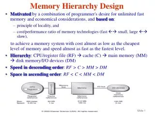
Introduction • The necessity of memory-hierarchy in a computer system design is enabled by the following two factors: • Locality of reference: The nature of program behavior • Large gap in speed between CPU and mass storage devices such a DRAM. • Level of memory hierarchy • High level <--- --> Low level • CPU Register, Cache, Main-memory, Disk • The levels of the hierarchy subset one another: all data in one level is also found in the level below.
Memory Hierarchy Difference between Desktops and Embedded Processors • Memory hierarchy for desktops • Speed • Memory hierarchy for Embedded Processors • Real-time applications need to care about worst-case performance. • Concerning about power consumption. • No memory hierarchy actually needed for simple and fix applications running on embedded processors. • Main memory itself may be quite small.
ABCs of Caches • Recalling some terms • Cache: The name given to the first level of the memory hierarchy encountered once the address leaves the CPU. • Miss rate: The fraction of accesses not in the cache. • Miss penalty: The additional time to service the miss. • Block: The minimum unit of information that can be present in the cache. • Four questions about any level of the hierarchy: • Q1: Where can a block be placed in the upper level? (Block placement) • Q2: How is a block found if it is in the upper level? (Block identification) • Q3: Which block should be replaced on a miss? (Block replacement) • Q4: What happens on a write? (Write strategy)
Cache Performance • Formula for performance evaluation • CPU execution time = (CPU clock cycles + Memory stall cycles) * Clock cycle time =IC *(CPIexecution + Memory stall clock cycles/IC)*Clock cycle time • Memory stall cycles = IC * Memory reference per instruction *miss rate *miss penalty • Measure of memory-hierarchy performance Average memory access time = Hit time + Miss rate * Miss penalty • Example on page 395. • Example on page 396.
Four Memory Hierarchy Questions Q1: Where can a block be placed in the upper level? ( block placement) Q2: How is a block found if it is in the upper level? ( block identification) Q3: Which block should be replaced on a miss? ( block replacement) Q4: What happens on a write? ( write strategy)
Block Placement (1) • Q1: Where can a block be placed in a cache? • Direct mapped: Each block has only one place it can appear in the cache. The mapping is usually (Block address) MOD (Number of blocks in cache) • Fully associative: A block can be placed anywhere in the cache. • Set associative: A block can be placed in a restricted set of places in the cache. A set is a group of blocks in the cache. A block is first mapped onto a set, and then the block can be placed anywhere within that set. The set is usually obtained by (block address) MOD (Number of sets in a cache) • If there are n blocks in a set, the cache is called n-way set associative.
Block Identification • Q2: How is a block found if it is in the cache • Each cache block consists of • Address tag: Give the block address • Valid bit: Indicate whether or not the associated entry contains a valid address. • Data • Relationship of a CPU address to the cache • Address presented by CPU • Block address ## Block offset • Index: Select the set • Block offset: Select the desired data from the block.
Identification Steps • Index field of the CPU address is used to select a set. • Tag field presented by the CPU is compared in parallel to all address tags of the blocks in the selected set. • If any address tag matches the tag field of the CPU address and its valid bit is true, it is a cache hit. • Offset field is used to select the desired data.
Associativity versus Index Field • If the total cache size is kept the same, • Increasing associativity increases the number of blocks per set, thereby decreasing the size of the index and increasing the size of the tag. • The following formula characterized this property: 2index = (cache size)/(block size *set associativity).
Block Replacement • Q3: Which block should be replaced on a cache miss? • For direct mapped cache, the answer is obvious. • For set associative or fully associative cache, the following two strategies can be used: • Random • Least-recently used (LRU) • First in, first out (FIFO)
Comparison of Miss Rate between Random and LRU • Fig. 5.6 on page 400
Write Strategy • Q4: What happens on a write? • Traffic patterns • “Writes” take about 7% of the overall memory traffic and take about 25% of the data cache traffic. • Though “read “ dominates processor cache traffic, “write” still can not be ignored in a high performance design. • “Read” can be done faster than “write” • In reading, the block data can be read at the same time that the tag is read and compared. • In writing, modifying a block cannot begin until the tag is checked to see if the address is a hit.
Write Policies and Write Miss Options • Write policies • Write through (or store through) • Write to both the block in the cache and the block in the lower-level memory. • Write back • Write only to the block in the cache. A dirty bit, attached to each block in the cache, is set when the block is modified. When a block is being replaced and the dirty bit is set, the block is copy back to main memory. This can reduce bus traffic. • Common options on a write miss • Write allocate • The block is loaded on a write miss, followed by the write-hit. • No-write allocate (write around) • The block is modified in the lower level and not loaded into the cache. • Either write miss option can be used with write through or write back, but write-back caches generally use write allocate and write-through cache often use no-write allocate.
Comparison between Write Through and Write Back • Write back can reduce bus traffic, but the content of cache blocks can be inconsistent with that of the blocks in main memory at some moment. • Write through increases bus traffic, but the content is consistent all the time. • Reduce write stall • Use a writing buffer. As soon as the CPU places the write data into the writing buffer, the CPU is allowed to continue. • Example on page 402
An Example: the Alpha 21264 Data Cache • Features • 64K bytes of data in 64-byte blocks. • Two-way set associative. • Write back with a dirty bit. • Write allocate on a write miss. • The CPU address • 48-bit virtual address • 44-bit physical address • 38-bit block address • 29-bit tag address • 9-bit index, obtained by 2index = 512= 65536/(64*2) • 6-bit block offset • FIFO replacement strategy • What happen on a miss? • 64-byte block is fetched from main memory in four transfer, each takes 5 clock cycles.
Unified versus Split Caches • Unified cache: A cache contains instructions and data. • Spit caches: Data is contained only in data cache, while instruction is contained in instruction cache. • Fig. 5.8 on page 406.
Cache Performance • Average memory access time for processors with in-order execution Average memory access time = Hit time + Miss rate * Miss penalty • Examples on pages 408 and 409 • Miss penalty and out-of-order execution processors Memory stall cycles / instruction = Misses/instruction * (Total miss latency – Overlapped miss latency) • Length of memory latency: Time between the start and the end of a memory reference in an out-of-order processor. • Length of latency overlap: A time period of memory latency overlapping the operations of the processor.
Improving Cache Performance • Reduce the miss rate • Reduce the miss penalty • Reduce the hit time • Reduce the miss penalty or miss rate via parallelism
Reducing Cache Miss Penalty • Multilevel caches • Critical word first and early restart • Giving priority to read misses over writes • Merging write buffers • Victim caches
Multilevel Caches • Question: • Larger cache or faster cache? A contradictory scenario. • Solution: • Adding another level of cache. • Second level cache complicates performance evaluation of cache memory. Average memory access time = Hit timeL1 + Miss rateL1 *Miss penaltyL1 Where, Miss penaltyL1 = Hit timeL2 + Miss rateL2 * Miss penaltyL2
Local and Global Miss Rates • The second-level miss rate is measured on the leftovers from the first-level cache. • Local miss rate (Miss rateL2) • The number of misses in the cache divided by the total number of memory accesses to this cache. • Global miss rate (Miss rateL1 *Miss rateL2) • The number of misses in the cache divided by the total number of memory accesses generated by the CPU.
Two Insights and Questions • Two insights from the observation of the results shown above: • The global cache miss rate is very similar to the single cache miss rate of the second-level cache. • The local cache miss rate is not a good measure of secondary caches; The global cache miss rate should be used because the effectiveness of second-level cache is a function of the miss rate of the first-level cache. • Two questions for the design of the second-level cache: • Will it lower the average memory access time portion of the CPI, and how much it cost?
Early Restart and Critical Word First • Basic idea: Don’t wait for the full block to be loaded before sending the requested word and restarting the CPU. • Two strategies: • Early restart: As soon as the requested word of the block arrives, send it to the CPU and let the CPU continue execution. • Critical word first: Request the missed word first from memory and send it to the CPU as soon as it arrives; let the CPU continue execution while filling the rest of the words in the block. • Example on page 419.
Given Priority to Read Miss over Writes • A write buffer can free the CPU from waiting for the completion of write, but it could hold the updated value of a location needed on a read miss. This complicates memory access, i.e., it may cause a RAW hazard. • Two solutions: • The read miss waits until the write buffer is empty. This certainly increases miss penalty. Or, • Check the contents of the write buffer on a read miss, and let the read miss fetch the data from the write buffer. • Example on page 419
Victim Caches (1) • Victim cache • A small fully associative cache contains only blocks that are discarded from a cache because of a miss -- “victim”. • The blocks of the victim cache is checked on a miss to see if they have the desired data before going to the next lower-level memory. If it is found there, the victim block and cache block are swapped. • A four entry victim cache can remove 20% to 95% of the conflict misses in a 4-KB direct mapped data cache.
Reducing Miss Rate • Larger block size • Larger caches • Higher associativity • Way prediction and psudoassociative caches • Compiler optimizations
Miss Categories • Compulsory miss • The first access to a block is not in the cache. • Capacity miss • Occur because of blocks being discarded and later retrieved if the cache cannot contain all the blocks needed during execution of a program. • Conflict miss • Occur because a block can be discarded and later retrieved if two many blocks map to its set for direct mapped or set associative caches. • What can a designer do with the miss rate? • Reduce conflict miss is the easiest: Fully associativity, but very expensive. • Reduce capacity miss: Use large cache. • Reduce compulsory miss: Use large block.
Larger Block Size • Reduce compulsory miss by taking advantage of spatial locality. • Increase miss penalty • Increase capacity miss if cache is small. • The selection of block size depends on both the latency and bandwidth of the lower-level memory: • High latency and high bandwidth encourages larger block sizes. • Low latency and low bandwidth encourages smaller block sizes. • Example on page 426.
Average Memory Access Time, Block Size versus Cache Size • Fig. 5.18 on page 428
Larger Caches • Drawbacks • Longer hit time • Higher cost
Higher Associativity • Two general rules of thumb • 8-way set associative is for practical purposes as effective in reducing misses as fully associative. • 2:1 cache rule of thumb • A direct mapped cache of size N has about the same miss rate as a 2-way set-associative cache of size N/2. • The pressure of a fast processor clock cycle encourages simple cache, but the increasing miss penalty rewards associativity • Example on page 429.
Average Memory Access Time versus Associativity • Fig. 5.19 on page 430