Download
1 / 40
410 likes | 437 Views
Learn the operation and applications of diodes, thyristors, and bipolar transistors as switches in this unit. Understand how to design a transistor switch, evaluate operational amplifier characteristics, and analyze amplifier circuits incorporating op-amps.

E N D
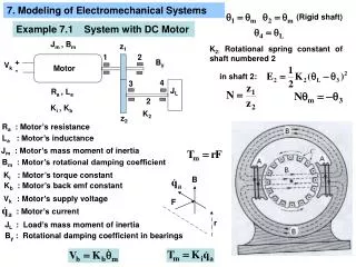
MM1 EM1 Electromechanical Systems Unit 3 Devices 1 1
Aim and Learning Outcomes 2 • This unit explains the basic operation of • Diodes • Thyristors • Bipolar transistors as a switch • Operational amplifier (op-amp)& its uses • After completing this unit you should be able to • Design a simple transistor switch. • Evaluate the basic characteristics of operational amplifiers • Analyse a variety of amplifiers, which incorporate op-amps
Content 3 3.1- Diode 3.2- Thyristor 3.3- Bipolar or Junction Transistor 3.4- Using the Transistor as a Switch 3.5- Operational Amplifiers 3.6- Inverting Amplifier 3.7- Summing Amplifier 3.8- Integrating Amplifier 3.9- Increasing the bandwidth 3.10- Unity Gain Amplifier 3.11- Input Resistance of Unity Gain Amplifier 3.12- Output Resistance of Unity Gain Amplifier 3.13- Non-inverting Amplifier
3.1 Diode P N 4
Open Circuit I = 0 ; V = Vd 6
Zener Diode LED Light Emitting Diode LDR Light Dependent Resistor 7
3.2 Thyristor • A solid-state semiconductor device with four layers of alternating N and P-type material. • The thyristor has a third terminal called the gate. 9
3.2 Thyristor • Reversed biased: It acts in a similar way to the diode (i.e. as an open circuit). • Forward biased: no current flows through it, until the gateis triggered by a small current pulse from an independent supply. • Once established the thyristor current continues until it falls to zero when it will be extinguished. • No further current will flow until the gate is triggered again 10
3.2 Thyristor 13 • Applications: • It is mainly used where high currents and voltages are involved, and are often used to control alternating currents, • It can be used as the control elements for phase angle triggered controllers, also known as phase fired controllers. • It can also be found in power supplies for digital circuits, where they can be used as a sort of "circuit breaker" or "crowbar" to prevent a failure in the power supply from damaging downstream components. • Types • SCR, Triac, Diac
3.2 Thyristor SCR can be used to form Full-wave rectified power control as shown below: 14
3.3 Bipolar or Junction Transistor • The bipolar transistor has three terminals • Base, • Collector and • Emitter • Types: PNP & NPN 15
3.3 Bipolar or Junction Transistor • For a transistor to conduct the collector – emitter voltage, VCE, must be positive and in excess of about 0.7 volts. • The collector current, ICE, is dependent on the magnitude of the base current, IB. • When the device is conducting the base – emitter voltage, VBE, remains virtually constant at 0.7 Volts. PNP-Type NPN-Type 16
3.3 Bipolar or Junction Transistor • Active Region: is the region normally employed for linear (undistorted) amplifiers. In the active region, the C-B junction is reverse-biased, while the B-E junction is forward-biased. • Cutoff Region: defined as that region where the collector current is 0A. In addition, the C-B and B-E junctions of a transistor are both reversed-biased in cutoff region. • Saturation Region: defined as that region of the characteristics to the left of VCB = 0V. The collector current increases exponentially as the voltage VCB increases toward 0V. In the saturation region, the C-B and B-E junctions are forward-biased. 18
3.4 Using the Transistor as a Switch • The voltage across the collector resistor RC, VRC = ICRC = VS - VCE • Slope = -1/RC • Intersects current IC axis at VS/RC • Crosses voltage VCE axis at VS • A suitable value for RC may be found from the transistor characteristics 19
Taking 12 Volts as a typical value for VS the intersection with the horizontal axis is marked. • A straight line (or “load line”) drawn so that it passes through the “knee” of the transistor characteristic curve. • By reading off the value of current where the load line crosses the vertical axis (i.e. VS/RC) RC can be calculated:- 20
The operating or Q (quiescent) point of the transistor. Quiescent or Ideal current and voltage present at the terminals of the device when DC supply is ON (biasing) For example:- • Operating at the point marked A. When IB = 0A IC will be very small, VCE will be almost equal to the supply voltage, VS Therefore, the transistor will be cut off (not conducting) and may be treated as an open circuit. 21
Operating at point B When IB approaches maximum value for the device (in this case 125A) IC will approach the maximum value for the device, VCE will be very small, the transistor will be saturated (acting like a conductor) and may be treated as a short circuit. 22
When the applied signal is positive: IB =100A increasing IC=3.1 mA and reducing VCE to 1.5 V. As the applied signal goes negative: IB =0A Reducing IC=0.5mA and Increasing VCE=10.3 V. At operating point D, • Without an input signal: • IB =50A, • IC, =1.8 mA and • VCE = VS – ICRC=5.9 Volts. • Change in IC >>IB transistor is a current amplifier. • +ve Vsignal IB and VCE. • Hence, the output voltage is the inverse of the input and the circuit is an inverting amplifier. 23
Large Input Signal • If applied signal is too large then it will cause the transistor to • Saturate on positive peaks and • Cut off on negative peaks • distorting the output voltage 25
Control panel switch open: • IB = 0 • IC very small • VCEVS • Transistor off • Control panel switch closed: • Ideally the transistor should be “hard” on and saturated • ICVS/RC To achieve this, the base current must be near the maximum for the device IBmax, requiring RB to be set equal to with VBE 0.7 Volts (constant) 26
3.5 The 741 OpAmp IC741 is a single chip (integrated circuit) containing 20 transistors, 11 resistors and 1 capacitor in one small package. 28
3.5 Operational Amplifiers • It is a linear amplifier • Used to perform basic arithmetic operations • Amplifies small signals 741 can be represented by a simple equivalent circuit that has: • Inverting input (-) • Non-Inverting input (+) • Output (only one). • –ve power supply pin • +ve power supply pin 29
Ri = input resistance, a very high value, which is normally assumed to be infinite • Ro = output resistance, a very low, which is normally assumed to be zero • A = open circuit voltage gain,ideally infinite. • Open circuit voltage gain varies with frequency. • Normally be operated only at frequencies where A > 103. 30
3.5 Ideal Op-Amp vL(t) = AvS(t) • The input circuit has equivalent resistance Rin, so that the input voltage, vin, is given by • The input voltage (seen by the amplifier) is amplified by a constant factor, A. • The voltage at the load is 31
3.5 Ideal Op-Amp vL(t) = AvS(t) • If the input resistance, Rin, were very large vin≈vS vin≈vS vL = Avin Thus, two desirable characteristics for a general-purpose voltage amplifier are a very large input impedance anda very small output impedance. 32
3.5 Ideal Op-Amp Ideal op-amp would have the following characteristic: • Infinite open-loop voltage gain, AOL • Infinite input impedance, Zin • Zero output impedance, Zout 0 • Infinite bandwidth, AOL remains unchanged from DC to very high frequency • Zero offset voltage, zero input (V+ = V-) produces zero output • Infinite common-mode rejection ratio, which only amplifies voltage difference between the two inputs 33
R 2 R 1 V – – V i V V + + o 3.6 Inverting Amplifier • If Ri is very large and the input current i0. • V|Ri is negligible and • V- 0(as it is called) at “virtual earth”. • With i 0, i2 = -i1 • With inverting input at virtual earth (i.e. V-0) Vi = i1R1 andVo = i2R2 Combining these equations gives Vri=0 So the overall gain The negative sign indicates that the output voltage is inverted, hence the name 34
3.6 Summing Amplifier We Know that V- 0(virtual earth) and i 0, if = -i1 Hence, -if = i1 + i2 + i3 If Rf = R1 = R2 = R3 Then, Vo = -[V1 + V2 + V3] Output voltage = -Input voltages 35
3.8 Integrating Amplifier We Know that V- 0, VC = Vo, i1 = -i2 and Substituting in the Integral equation gives: If Viis constant, Thus Output voltage is to the integral of the input voltage 36
3.8 Unity Gain Amplifier • If Rs=Rout=0, VL=Vi =0 =0 A=1 Vo is a copy of Vi Commonly used in instrumentation systems to interface transducers and recording instruments Also known as the Voltage Follower or Buffer Amplifier 37
Vo = Av = A(V+ - V-) = A(Vi – Vo) The “equivalent voltage generator”, Avi, Vo(1 + A) = AVi A >> 1, so 38
3.12 Non-Inverting Amplifier Show that the Voltage gain is 43
Conclusion 44 This unit explains the basic operation of • Diodes • Thyristors And used them as Wave Rectifiers • Bipolar transistors as: • Switch and • Amplifier • Operational amplifier (op-amp)& its uses • Inverter • Integrator • Follower