Download
1 / 15
310 likes | 1.81k Views
8-Bit Barrel Shifter. Cyrus Thomas Ekemini Essien Kuang-Wai (Kenneth) Tseng Advisor: Dr. David Parent December 8, 2004. Agenda. Abstract Introduction Why Simple Theory Back Ground information (Lit Review) Summary of Results Project (Experimental) Details Results Cost Analysis

E N D
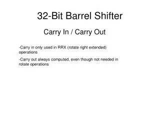
8-Bit Barrel Shifter Cyrus Thomas Ekemini Essien Kuang-Wai (Kenneth) Tseng Advisor: Dr. David Parent December 8, 2004
Agenda • Abstract • Introduction • Why • Simple Theory • Back Ground information (Lit Review) • Summary of Results • Project (Experimental) Details • Results • Cost Analysis • Conclusions
Abstract • Designed and Verified an 8-bit Barrel Shifter that operates at 200 MHz, uses 15.39 mW of Power, occupies an area of 340 x 300 m2 and has a power density of 15.1 W/cm2. • The shifter works by shifting the bits left. • Inputs: Data bits D0-D7 & encoded Select lines S2, S1, S0. • Outputs: Shifted Data bits Q0 – Q7. • Implementation Technology : 0.6 micron process. • Latency = 5n s. • External load driving capability = 33f F. • Number of Metal layers used = 3.
Introduction • Because there were 5 stages (combining each flip flop stage as one stage), the propagation delay time was divided amongst all 5 stages with each stage having a different driving capacitance. • Since each output of multiplexer in stage 2 and 3 was connected to 2 other multiplexers, the fan out was 2. • Since the connection from the multiplexers have long wires through out the circuit, parasitic capacitances were considered for sizing.
8 Bit Barrel Shifter Logic Diagram Stage 3 Stage 4 Stage 5 Stage 1 Stage 2
Project Summary • We designed a 8 bit Barrel Shifter that shifts data from an input to an output depending on the combination of three select lines. • Our design of the Barrel shifter allows for an increase in the number of input bits without having to modify the existing design. • Our design met the specifications for the project.
Longest Path Calculations Note: All widths are in microns and capacitances in fF
Cost Analysis • We had to invest our time and resources to complete this project. By our estimation, considering that we also had to study for other classes, we spent • 12 hours worth of time in a week and a half looking for and deciding on a project with Dr. Parent’s consent. • 8 hours worth of time in a week verifying our logic and making our schematic. • 6 hours worth of time in a day verifying our timing. • 36 hours worth of time in two and half weeks making the layout of our project. • 8 hours of time in a week in determining our post extraction time.
Lessons Learned • Doing the project helps in better understanding the course material. • Start the project on time as the earlier you start, the better. • Consult with the course instructor (Dr. Parent in this case) and your peers whenever you get stuck on the project as no one can know it all. • And most importantly view the project as an opportunity to have fun while learning. It will make it a worthwhile experience.
Summary • Our project was a worthwhile endeavor as not many people know what a barrel shifter is and what it is used for. As such, doing it and presenting it to the class has helped to enlighten our classmates. • Most importantly we got our circuit design to work and meet specification as we have ably shown in our presentation. • We believe that our circuit can become a stepping stone to improving computer organization and memory.
Acknowledgements • Thanks to each member of the group for putting up with one another. • Thanks to Cadence Design Systems for the VLSI lab • Thanks to Synopsys for Software donation • Thanks to Professor Parent for his assistance and advising with the project. • Thanks to you all for listening.