8 Bit ALU
8 Bit ALU. Rahul Vyas Gyanesh Chhipa Jaimin Shah Advisor: Dr. David W. Parent 05/08/2006. Abstract. The 8-bit ALU that our group designed can perform 8 arithmatic function and 4 logic function The 8s-bit ALU is made up of 2 identical 4-bit ALU, and 25 DFFs.

8 Bit ALU
E N D
Presentation Transcript
8 Bit ALU Rahul Vyas Gyanesh Chhipa Jaimin Shah Advisor: Dr.David W. Parent 05/08/2006
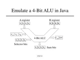
Abstract • The 8-bit ALU that our group designed can perform 8 arithmatic function and 4 logic function • The 8s-bit ALU is made up of 2 identical 4-bit ALU, and 25 DFFs. • We designed an 8-bit carry look ahead adder that operated at 200 MHz
Introduction • An ALU is the fundamental unit of any computing system. • Understanding how an ALU is designed and how it works is essential to building any advanced logic circuits. • Using this knowledge and experience, we can move on to designing more complex integrated circuits. • Design consists of different kinds of logic… Look ahead carry generator, adder, Subtractor, Transfer Data, DFF, Multiplexer, Inv, and, Xor, etc
Project Summary • Created Schematic • Tested the schematics logic by using NCVerilog. • Finding longest path • Sizing of Wn and Wp • Layout of individual block • Checked DRC and LVS for each block • Integrated every block • Checked DRC and LVS for final layout • Verify the timing • Measure power
Block diagram of our project ARITHMETIC CIRCUIT DFF’S DFF’S MUX LOGICAL CIRCUIT
[1]SELECTION OUTPUT FUNCTION S2 S1 S0 CIN 0 0 0 0 F=A Transfer A 0 0 0 1 F=A+1 Increment A 0 0 1 0 F=A+B Addition 0 0 1 1 F=A+B+1 Add with Carry 0 1 0 0 F=A-B-1 Substract with Borrow 0 1 0 1 F=A-B Substraction 0 1 1 0 F=A-1 Decrement A 0 1 1 1 F=A Transfer A 1 0 0 X F=AB OR 1 0 1 X F=AB XOR 1 1 0 X F=AB AND 1 1 1 X F=Ā Complement A Project Details [1] A=B=8 Bit Inputs. S2 S1,S0,CIN:-Selection Lines
Longest Path Calculations Note: All widths are in Cm and capacitances in fF Tphl = 5ns/19 = 0.263ns
Verification LVS The net lists matched
Cost Analysis • verifying logic: 2 weeks • verifying timing: 1 week • Layout: 1weeks • post extracted timing: 5 days
Lessons Learned • Aspects of design processes • Simulation and verification tools • Optimize transistor size to meet specification • Use instances • See Dr. Parent more often to understand the concept fully.
Summary Project: • Our 8-Bit ALU has 1520 transistors and 33 terminals. • The circuit can operate up to 250MHz. • Designed a 8-Bit ALU that performs eight arithmetic and four logical functions at 200MHz frequency with setup and hold time 1ns, driving up to 30fF. • This circuit can be used as a building block for 16/32-bit ALU. • The Logic design can be modified to perform more functions.
Acknowledgements • Thanks to Professor David Parent for his Guidance And Help • Thanks to Cadence Design Systems for the VLSI lab