Download
1 / 17
170 likes | 187 Views
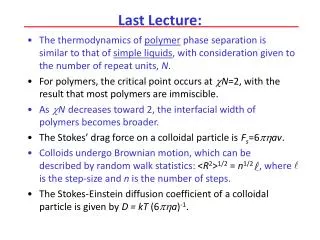
Recall Last Lecture. Voltage Transfer Characteristic A plot of V o versus V i Use BE loop to obtain a current equation, I B in terms of V i Use CE loop to get I C in terms of V o Change I C in terms of I B Equate the two equations to link V i with V o. V o (V). Cutoff. 5. = 4.8.

E N D
Recall Last Lecture • Voltage Transfer Characteristic • A plot of Vo versus Vi • Use BE loop to obtain a current equation, IB in terms of Vi • Use CE loop to get IC in terms of Vo • Change IC in terms of IB • Equate the two equations to link Vi with Vo
Vo (V) Cutoff 5 = 4.8 Active 0.2 Saturation x 5 x Vi (V) = 4.3 0.7
Bipolar Transistor Biasing • Biasing refers to the DC voltages applied to the transistor for it to turn on and operate in the forward active region, so that it can amplify the input AC signal
Proper Biasing Effect Ref: Neamen
Effect of Improper Biasing on Amplified Signal Waveform Ref: Neamen
Three types of biasing • Fixed Bias Biasing Circuit • Biasing using Collector to Base Feedback Resistor • Voltage Divider Biasing Circuit
Biasing Circuits – Fixed Bias Biasing Circuit • The circuit is one of the simplest transistor circuits is known as fixed-bias biasing circuit. • There is a single dc power supply, and the quiescent base current is established through the resistor RB. • The coupling capacitor C1acts as an open circuit to dc, isolating the signal source from the base current. • Typical values of C1 are in the rage of 1 to 10 μF, although the actual value depends on the frequency range of interest.
Example – Fixed Bias Biasing Circuit Determine the following:(a) IB and IC(b) VCE(c) VB and VC NOTE: Proposed to use branch current equations and node voltages
Biasing using Collector to Base Feedback Resistor Find RB and RC such that IE = 1mA , VCE = 2.3 V, VCC = 10 V and b=100. IC + IB = IE IB IC IE NOTE: Proposed to use branch current equations and node voltages
Biasing using Collector to Base Feedback Resistor IE = 1mA , VCE = 2.3 V, VCC = 10 V and b=100. • (VC – VB ) / RB= IB • but VC = VCE • and VB = VBE = 0.7 V • (2.3 – 0.7) / RB = (IE / (b+1) • RB = 161.6 kW • (VCC – VC ) / RC = IE • RC = 7.7 kW VC VB
Voltage Divider Biasing Circuit This is a very stable bias circuit. The currents and voltages are almost independent of variations in .
Analysis Redrawing the input side of the network by changing it into Thevenin Equivalent RTh: the voltage source is replaced by a short-circuit equivalent
VTH VTH Analysis VTh: open-circuit Thevenin voltage is determined. Inserting the Thevenin equivalent circuit Use voltage divider
Analysis The Thevenin equivalent circuit
BJT Biasing in Amplifier Example • Find VCE ,IE, IC and IBgiven • b=100, VCC=10V, R1 = 56 kW, R2 = 12.2 kW, • RC = 2 kW andRE = 0.4 kW • VTH= R2 /(R1 + R2)VCC • VTH = 12.2k/(56k+12.2k).(10) • VTH = 1.79V • RTH = R1 // R2 • = 10 kW
BJT Biasing in Amplifier Circuits • VTH = RTH IB + VBE + RE IE • 1.79= 10k IB + 0.7+ 0.4k (b+1)IB • IB = 21.62mA • IC = bIB= 100(21.62m)=2.16mA • IE = IC + IB = 2.18mA • VCC = RC IC + VCE + RE IE • 10 = 2k(2.16m)+VCE +0.4(2.18m) • VCE = 4.8 V