Download
1 / 17
170 likes | 177 Views
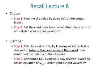
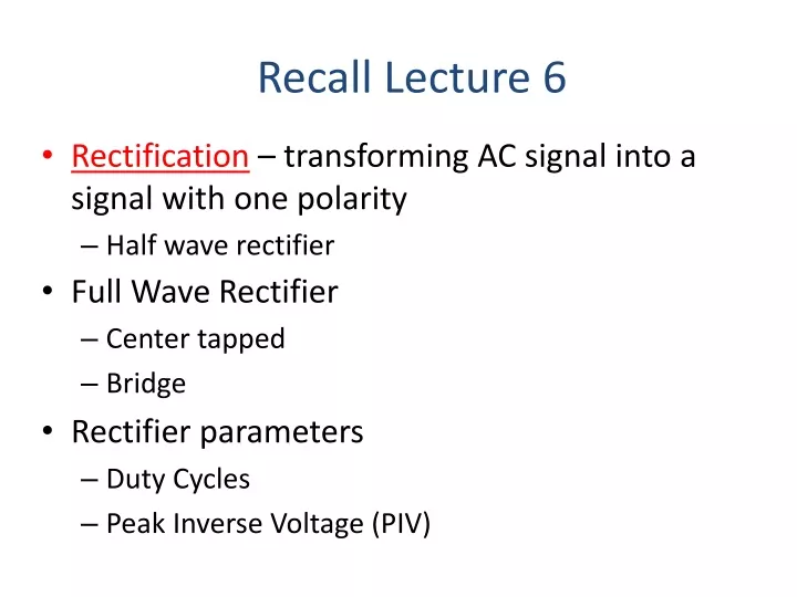
Recall Lecture 6. Rectification – transforming AC signal into a signal with one polarity Half wave rectifier. Full Wave Rectifier Center tapped Bridge Rectifier parameters Duty Cycles Peak Inverse Voltage (PIV). Clipper Circuits. V’ = V B + V . Standard Clipper Circuits.

E N D
Recall Lecture 6 • Rectification – transforming AC signal into a signal with one polarity • Half wave rectifier • Full Wave Rectifier • Center tapped • Bridge • Rectifier parameters • Duty Cycles • Peak Inverse Voltage (PIV)
V’ = VB + V Standard Clipper Circuits • Clipper circuits, also called limiter circuits, are used to eliminate portion of a signal that are above or below a specified level – clip value. • The purpose of the diode is that when it is turn on, it provides the clip value • Find the clip value = V’. To find V’, use KVL at L1 assuming the diode is on • The equation is : V’ – VB - V = 0 V’ = VB + V • iii. Then, set the conditions • If VI > V’, what happens? diode conducts, clips and hence Vo = V’ • If VI < V’, what happens? diode off, open circuit, no current flow, Vo = Vi VI L1
EXAMPLE For the circuit shown below sketch the waveform of the output voltage, Vo. The input voltage is a sine wave where VI = 5 sin t. VB is given as 1.3 V. Assume V = 0.6 V 1.3 V
V’ = 1.9V Solution • Find the clip value = V’. To find V’, use KVL at L1 assuming the diode is on • The equation is : V’ – 1.3 - 0.6= 0 V’ = 1.9 V • iii. Then, set the conditions • If Vin > V’, what happens? diode conducts, clips and hence Vo = V’ = 1.9 V • If Vin < V’, what happens? diode off, open circuit, no current flow, Vo = Vi 1.3 V VI
EXAMPLE For the circuit shown below sketch the waveform of the output voltage, Vout. The input voltage is a sine wave where Vin = 10 sin t. Assume V = 0.7 V + Vout - + Vin -
V’ = 3.3V Solution • Find the clip value = V’. To find V’, use KVL at L1 assuming the diode is on • The equation is : V’ – 4 + 0.7= 0 V’ = 3.3 V • iii. Then, set the conditions • If Vin > V’, what happens? diode off, open circuit, no current flow, Vo = Vi • If Vin < V’, what happens? diode conducts, clips and hence Vo = V’ = 3.3 V VI L1
Parallel Based Clippers • Positive and negative clipping can be performed simultaneously by using a double limiter or a parallel-based clipper. • The parallel-based clipper is designed with two diodes and two voltage sources oriented in opposite directions. • This circuit is to allow clipping to occur during both cycles; negative and positive
Clipper in Series c b a Initial stage: node a = 0V Hence, node b = 1.5 V So, node c of the diode must be at least 2.2 V ECE 1201 The input signal is an 8 V p-p square wave. Assume, V = 0.7 V. Sketch the output waveform, Vo.
Hence, the positive cycle of the square wave has met the condition of 2.2 V • Perform KVL as usual: – 4 + 0.7 + 1.5 + Vo= 0 Vo = 1.8 V 4 1.8 -4
What if now the input is change to 4 sin t? • It has to wait for the input signal to reach 2.2 V. Before that, the output, Vo is zero as diode is off. • Perform KVL as usual: – 4 + 0.7 + 1.5 + Vo= 0 Vo = 1.8 sin t V
So, basically, clipper in series clips at zero. It is similar to half wave where the diode only turns on during one of the cycle.
Clipper in Series a c b P3.11(a) P3.11(b) Initial stage: node a = 0V Hence, node b = - 0.7 V So, node c of the diode must be at least -1.9 V Problem 3.11 Figure P3.11(a) shows the input voltage of the circuit as shown in Figure P3.11(b). Plot the output voltage Vo of these circuits if V = 0.7 V
Hence, the negative cycle of the square wave has met the condition of |1.9| V • Perform KVL as usual: + 3 - 0.7 - 1.2 + Vo= 0 Vo = - 1.1 V vo - 3V + -1.1 -1.1
What if now the input is change to 5 sin t ? • It has to wait for the input signal (negative cycle) to reach |1.9| V. Before that, the output, Vo is zero as diode is off. • Perform KVL as usual: + 5 - 0.7 - 1.2 + Vo= 0 Vo = -3.1 sin t V