Download
1 / 16
160 likes | 175 Views
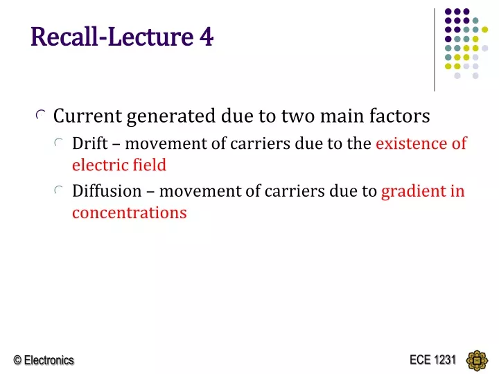
Recall-Lecture 4 . Current generated due to two main factors Drift – movement of carriers due to the existence of electric field Diffusion – movement of carriers due to gradient in concentrations. Recall-Lecture 4 . Introduction of PN junction Space charge region/depletion region

E N D
Recall-Lecture 4 • Current generated due to two main factors • Drift – movement of carriers due to the existence of electric field • Diffusion – movement of carriers due to gradient in concentrations
Recall-Lecture 4 • Introduction of PN junction • Space charge region/depletion region • Built-in potential voltage Vbi • Reversed biased pn junction • no current flow • Forward biased pn junction • current flow due to diffusion of carriers.
CIRCUIT REPRESENTATION OF DIODE – Ideal Model VD = - VS Reverse-bias I-V characteristics of ideal model Forward-bias
EXAMPLE: Determine the diode voltage and current in the circuit using ideal model for a silicon diode. Also determine the power dissipated in the diode.
CIRCUIT REPRESENTATION OF DIODE – Piecewise Linear Model VD = - VS Reverse-bias I-V characteristics of constant voltage model Forward-bias
EXAMPLE: Determine the diode voltage and current in the circuit (using constant voltage model) for a silicon diode. Also determine the power dissipated in the diode. Consider the cut-in voltage V = 0.65 V.
CIRCUIT REPRESENTATION OF DIODE – Piecewise Linear Model VD = - VS Reverse-bias I-V characteristics of piecewise model Forward-bias
EXAMPLE: Determine the diode voltage and current in the circuit using piecewise linear model for a silicon diode. Also determine the power dissipated in the diode. Consider the cut-in voltage V = 0.65 V and the diode DC forward resistance, rf = 15 Ω.
Diode Circuits: Direct Approach Question Determine the diode voltage and current for the circuit. Consider IS = 10-13 A. VPS = IDR + VD 5 = (2 x 10³) (10-13) [ e ( VD / 0.026) – 1 ] + VD VD = 0.619 V And ID = 2.19 mA ITERATION METHOD
DC Load Line • A linear line equation • ID versus VD • Obtain the equation using KVL
The value of ID V Use KVL: 2ID + VD – 5 = 0 ID = -VD + 5 = - VD + 2.5 2 2
EXAMPLE A diode circuit and its load line are as shown in the figure below Design the circuit when the diode is operating in forward bias condition. Determine the diode current ID and diode forward resistancerf in the circuit using a piecewise linear model. Consider the cut-in voltage of the diode, Vγ = 0.65V.
at VD = 0.7V ID = (5 – 0.7) / 2 = 2.15 mA Now, VD = Vγ + ID rf 0.7 = 0.65 + 2.15 rf rf = 0.05 / 2.15 mA = 23. 3 Ω IDR + VD – 5 = 0 ID = -VD/R + 5/ R 5/ R = 2.5 mA R = 2 kΩ