Download
1 / 23
230 likes | 415 Views
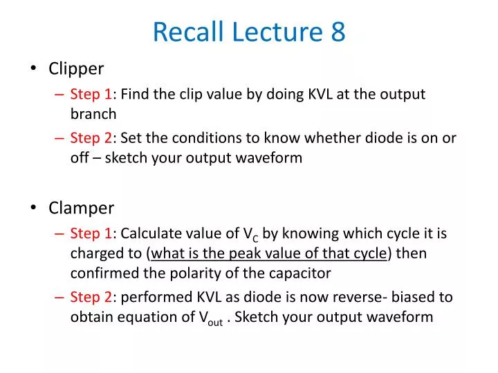
Recall Lecture 8. Clipper Step 1 : Find the clip value by doing KVL at the output branch Step 2 : Set the conditions to know whether diode is on or off – sketch your output waveform Clamper

E N D
Recall Lecture 8 • Clipper • Step 1: Find the clip value by doing KVL at the output branch • Step 2: Set the conditions to know whether diode is on or off – sketch your output waveform • Clamper • Step 1: Calculate value of VC by knowing which cycle it is charged to (what is the peak value of that cycle) then confirmed the polarity of the capacitor • Step 2: performed KVL as diode is now reverse- biased to obtain equation of Vout . Sketch your output waveform
REMEMBER THAT: A pn junction diode will conduct when the p-type material is more positive than the n-type material
OR GATE Vo = voltage across R
AND GATE Vo = node voltage
e e e h h h REMEMBER THIS Current flow in the opposite direction of the electrons flow; same direction as holes I
Transistor Structures • The bipolar junction transistor (BJT) has three separately doped regions and contains two pn junctions. • Bipolar transistor is a 3-terminal device. • Emitter (E) • Base (B) • Collector (C) • The basic transistor principle is that the voltage between two terminals controls the current through the third terminal. • Current in the transistor is due to the flow of both electrons and holes, hence the name bipolar.
Transistor Structures • There are two types of bipolar junction transistor: npn and pnp. • The npn bipolar transistor contains a thin p-region between two n-regions. • The pnp bipolar transistor contains a thin n-region sandwiched between two p-regions.
3 Regions of Operation • Active Operating range of the amplifier. Base-Emitter Junction forward biased. Collector-Base Junction reverse biased • Cutoff The amplifier is basically off. There is voltage but little current. Both junctions reverse biased • Saturation The amplifier is full on. There is little voltage but lots of current. Both junctions forward biased
C B E OPERATIONS - npn ACTIVE MODE + VBE • The base-emitter (B-E) junction is forward biased and the base-collector (C-B) junction is reverse-biased,. - • Since the B-E junction is forward biased, electrons from the emitter are injected across the B-E junction into the base IE • Once in the base region, the electrons are quickly accelerated through the base due to the reverse-biased C-B region IC iB • Some electrons, in passing through the base region, recombine with majority carrier holes in the base. This produces the current IB
TO ILLUSTRATE E B C - VBE + • Imagine the marbles as electrons • A flat base region with gaps where the marbles may fall/trapped – recombine • A sloping collector region represents high electric field in the C-B region • Hence, when enough energy is given to the marbles, they will be accelerated towards to base region with enough momentum to pass the base and straight ‘fly’ to the collector
C + VBE - B E MATHEMATICAL EXPRESSIONS IC IB IE IE = IS [ e VBE / VT -1 ] = IS e VBE / VT Based on KCL: IE = IC + IB No. of electrons crossing the base region and then directly into the collector region is a constant factor of the no. of electrons exiting the base region IC = IB No. of electrons reaching the collector region is directly proportional to the no. of electrons injected or crossing the base region. Ideally = 1, but in reality it is between 0.9 and 0.998. IC = IE
Based on KCL: IE = IC + IB IC = IB IC = IE IE = IB + IB = IB(+ 1) IE = IB(+ 1) Now With IC = IB IB = IC / Hence, IE = [ IC / ](+ 1) IC = IE[ / + 1 ] Comparing with IC = IE = [ / + 1 ]
C B E OPERATIONS - pnp IB IC FORWARD ACTIVE MODE - • The emitter – base (E- B) junction is forward biased and the base-collector (B- C) junction is reverse-biased,. VEB IE + IE = IS [ e VEB / VT -1 ] = IS e VEB / VT **Notice that it is VEB Based on KCL: IE = IC + IB
SUMMARY: Circuit Symbols and Conventions Based on KCL: IE = IC + IB npn bipolar transistor simple block diagram and circuit symbol. Arrow is on the emitter terminal that indicates the direction of emitter current (out of emitter terminal for the npn device) pnp bipolar transistor simple block diagram and circuit symbol. Arrow is on the emitter terminal that indicates the direction of emitter current (into of emitter terminal for the pnp device)
EXAMPLE 4.1 Calculate the collector and emitter currents, given the base current and current gain. Assume a common-base current gain and a base current of . Also assume that the transistor is biased forward in the forward active mode. Solution: The common-emitter current gain is The collector current is And the emitter current is
Common-Emitter Configuration - npn • The Emitter is common to both input (base-emitter) and output (collector-emitter). • Since Emitter is grounded, VC = VCE • With decreasing VC (VCE), the junction B-C will become forward biased too. • The current IC quickly drops to zero because electrons are no longer collected by the collector NodeB 0V
Characteristics of Common-Emitter - npn NOTE: VEC for PNP
EXAMPLE 1 Given IB = 6.0A and IC=510 A Determine , and IE EXAMPLE 2 NPN Transistor Reverse saturation current Is = 10-13A with current gain, = 90. Based on VBE = 0.685V, determine IC , IB and IE Examples • EXAMPLE 3 • PNP Transistor • = 60, IC= 0.85mA • Determine , IE and IB