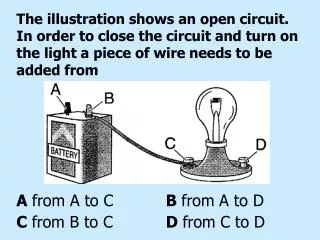
Download
1 / 24
240 likes | 388 Views
AID–EMC: Low Emission Digital Circuit Design. Update of the “Digital EMC project”. March 1st, 2006. Junfeng Zhou Wim Dehaene KULeuven ESAT-MICAS. Outline. Test chip finished 2. Theoretical analysis 3. Chip Testing proposal. Test layout for EMI regulator done.

E N D
AID–EMC: Low Emission Digital Circuit Design Update of the “Digital EMC project” March 1st, 2006 Junfeng Zhou Wim Dehaene KULeuven ESAT-MICAS
Outline Test chip finished 2. Theoretical analysis 3. Chip Testing proposal
Test layout for EMI regulator done • Layout transferred end of january, to be integrated in complete test chip. • Taped out is/was when? • One last change …
Last change of the layout add extra output pin Vcontrol Using metal 5 (can be cut in case of trouble) Making measurements more flexible Shaping the TF according to the values of Caux and Raux
Outline Test chip finished 2. Theoretical analysis 3. Chip Testing proposal
Simplified model p1 z1 p3 p2 • 4 nodes, difficult to analyze
Simplified model p1 Iout Ii Vi p3 p2 Short to ground
Stability analysis - Small signal analysis Approximation: p1 dominant pole second pole z1 High frequency pole p2 p3 High frequency , left half-plane zero Gain of the current source Stability ~ Caux/Ctank >3 for > 72° phase margin
Stability analysis – Simulation vs. Calculation Iload =192.7u A φ>72° φ>72° Stability vs. Iload Maple calculation Spectre simulation Raux=1.852K , Caux=20p,Ctank=100p
Current TF analysis H(s)=Idd(s)/Iin(s) dominant pole second pole third pole High frequency zero left half-plane zero
Current TF- simulation vs. calculation Maple calculation Spectre simulation Infinite Attenuation ?? Not in reality! Iload =80u A, Raux=1.852K , Ctank=100p
Model revisited Cdb1 p1 z1 p3 p2
Current TF- simulation vs. calculation TF vs. Caux Maple calculation Spectre simulation Iload =80u A, Raux=1.852K , Ctank=100p
Maximum Attenuation TF vs. Caux Cut off freq. ~ 1/Caux Large attenuation requires Large Ctank and/or small Cdb1 Cascode structure ! Maple calculation Iload =80u A, Raux=1.852K , Ctank=100p
Caux/Ctank and time domain ∆Vdd • Equations to be calculated • However:∆Vdd ~ Caux/Ctankin damped case ∆Vdd Caux = 1..5 pF
Conclusion • Regulator design criteria for Caux,Ctank • Stability ~ Caux/Ctank • Current transfer function (i.e. di/dt attenuation) • Cut off freq: Gm/Caux • Max. attenuation: Cdb1/(Cdb1+Ctank) • Time domain ∆Vdd • Caux/Ctank • Conclusion • Caux/Ctank determines stability and ∆Vdd. More stable also means a larger ∆Vdd ! • Design for small Cdb1 • Similar story possible for Gm, Gm1
Chip Testing proposal Test: List of tests for di/dt Test setup proposal To be designed => test board 3. Will we also do the emission tests ?
List of tests for di/dt • For the special EMC regulator: • Current pulse measurement, • 2. The current TF as a function of Ctank, Caux • 3. Measurement of di/dt reduction vs. Ctank, Caux and decoupling cap, • 4. Influence of different loads provided by AMIS • -- D-FF or MS-FF • -- number of gates • -- distributed clocks over time • ……
Test setup for di/dt measurement 1. For di/dt transient measurement • DUT is • EMI regulator • EMI regulator + V-regulator 1. OPAMP, BW ? 2. Current probe ? 3. Transformer ?
Test setup for Transfer function 2. For Transfer Function measurement
Design of Test Board 1. OPAMP, BW ? 2. Current probe ? 3. Transformer ? To be designed …
Measurement of Emission IEC 61967-4 International Standard IEC 61967-2 International Standard Chip under test Spectrum Analyzer IC Inner side Outer side 1 Ohm radiated mode conducted mode Do we need to measure this? How ? 1/150 ohm method can be foreseen on testboard
Future work 1. • Test board ?, • Chip measurement, • Finish the theoretical analysis, 2. • Continue research on the Clock strategy: SSCG
Questions Thank you for your attention