Digital Design Flow
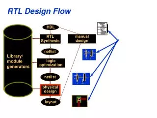
Digital Design Flow. Digital Design Flow begins with specification of the design at various levels of abstraction. Design entry phase: Specification of design as a mixture of behavioral Verilog code, instantiation of Verilog modules, and bus and wire assignments. Digital Design Flow.

Digital Design Flow
E N D
Presentation Transcript
Digital Design Flow • Digital Design Flow begins with specification of the design at various levels of abstraction. • Design entry phase: Specification of design as a mixture of behavioral Verilog code, instantiation of Verilog modules, and bus and wire assignments Verilog Digital System Design Z. Navabi, 2006
Digital Design Flow • FPLD Design Flow Verilog Digital System Design Z. Navabi, 2006
Digital Design Flow Design Entry Phase • FPLD Design Flow Verilog Digital System Design Z. Navabi, 2006
Digital Design Flow • Presynthesis verification: Generating testbenches for verification of the design and later for verifying the synthesis output Verilog Digital System Design Z. Navabi, 2006
Digital Design Flow Presynthesis Verification • FPLD Design Flow (Continued) Verilog Digital System Design Z. Navabi, 2006
Digital Design Flow • Synthesis process: Translating the design into actual hardware of a target device (FPLD, ASIC or custom IC) Verilog Digital System Design Z. Navabi, 2006
Digital Design Flow Synthesis Process • FPLD Design Flow (Continued) Verilog Digital System Design Z. Navabi, 2006
Digital Design Flow • Postsynthesis simulation: Testing the behavioral model of the design and its hardware model by using presynthesis test data Verilog Digital System Design Z. Navabi, 2006
Digital Design Flow Postsynthesis Verification • FPLD Design Flow (Continued) Verilog Digital System Design Z. Navabi, 2006
Digital Design Flow • Digital Design Flow ends with generating netlist for an application specific integrated circuits (ASIC), layout for a custom IC, or a program for a programmable logic devices (PLD) Verilog Digital System Design Z. Navabi, 2006
Digital Design Flow • FPLD Design Flow (Continued) Verilog Digital System Design Z. Navabi, 2006
Digital Design Flow Verilog Digital System Design Navabi, 2006
Verilog HDL • A language that can be understood by: • System Designers • RT Level Designers, • Test Engineers • Simulators • Synthesis Tools • Machines • Has become an IEEE standard Verilog Digital System Design Z. Navabi, 2006
The Verilog Language • The Verilog HDL satisfies all requirements for design and synthesis of digital systems: • Supports hierarchical description of hardware from system to gate or even switch level. • Has strong support at all levels for timing specification and violation detection. • A hardware component is described by the module_declaration language construct in it. Verilog Digital System Design Z. Navabi, 2006
The Verilog Language • The Verilog HDL satisfies all requirements for design and synthesis of digital systems (Continued): • Description of a module specifies a component’s input and output list as well as internal component busses and registers within a module, concurrent assignments, component instantiations, and procedural blocks can be used to describe a hardware component. • Several modules can hierarchically be instantiated to form other hardware structure. • Simulation environments provide graphical front-end programs and waveform editing and display tools. • Synthesis tools are based on a subset of Verilog. Verilog Digital System Design Z. Navabi, 2006
Elements of Verilog • We discuss basic constructs of Verilog language for describing a hardware module. Verilog Digital System Design Z. Navabi, 2006
Elements of Verilog Verilog Digital System Design Z. Navabi, 2006
Hardware Modules Verilog Digital System Design Z. Navabi, 2006
Hardware Modules module : The Main Component of Verilog Keyword module module module-name List of ports; Declarations ... Functional specification of module ... endmodule Variables, wires, and module parameters are declared. Keyword endmodule • Module Specifications Verilog Digital System Design Z. Navabi, 2006
Hardware Modules • There is more than one way to describe a Module in Verilog. • May correspond to descriptions at various levels of abstraction or to various levels of detail of the functionality of a module. • We show a small example and several alternative ways to describe it in Verilog. Verilog Digital System Design Z. Navabi, 2006
Primitive Instantiations Verilog Digital System Design Z. Navabi, 2006
Primitive Instantiations Logic Gates called Primitives • A Multiplexer Using Basic Logic Gates Verilog Digital System Design Z. Navabi, 2006
Primitive Instantiations module MultiplexerA (input a, b, s, output w); wire a_sel, b_sel, s_bar; not U1 (s_bar, s); and U2 (a_sel, a, s_bar); and U3 (b_sel, b, s); or U4 (w, a_sel, b_sel); endmodule Instantiation of Primitives • Primitive Instantiations Verilog Digital System Design Z. Navabi, 2006
Assign Statements Verilog Digital System Design Z. Navabi, 2006
Assign Statements Continuously drives w with the right hand side expression module MultiplexerB (input a, b, s, output w); assign w = (a & ~s) | (b & s); endmodule Using Boolean expressions to describe the logic • Assign Statement and Boolean Verilog Digital System Design Z. Navabi, 2006
Condition Expression Verilog Digital System Design Z. Navabi, 2006
Condition Expression Can be used when the operation of a unit is too complex to be described by Boolean expressions module MultiplexerC (input a, b, s, output w); assign w = s ? b : a; endmodule • Assign Statement and Condition Operator Very Effective in describing complex functionalities Useful in describing a behavior in a very compact way Verilog Digital System Design Z. Navabi, 2006
Procedural Blocks Verilog Digital System Design Z. Navabi, 2006
Procedural Blocks always statement Sensitivity list module MultiplexerD (input a, b, s, output w); reg w; always @(a, b, s) begin if (s) w = b; else w = a; end endmodule Can be used when the operation of a unit is too complex to be described by Boolean or conditional expressions if-else statement • Procedural Statement Verilog Digital System Design Z. Navabi, 2006
Module Instantiations Verilog Digital System Design Z. Navabi, 2006
Module Instantiations module ANDOR (input i1, i2, i3, i4, output y); assign y = (i1 & i2) | (i3 & i4); endmodule // module MultiplexerE (input a, b, s, output w); wire s_bar; not U1 (s_bar, s); ANDOR U2 (a, s_bar, s, b, w); endmodule ANDOR module is defined ANDOR module is instantiated • Module Instantiation Verilog Digital System Design Z. Navabi, 2006
Module Instantiations • Multiplexer Using ANDOR Verilog Digital System Design Z. Navabi, 2006
Component Description in Verilog Verilog Digital System Design Z. Navabi, 2006
Data Components Verilog Digital System Design Z. Navabi, 2006
Data Components Verilog Digital System Design Z. Navabi, 2006
Multiplexer Multiplexer Verilog Digital System Design Z. Navabi, 2006
Multiplexer Defines a Time Unit of 1 ns and Time Precision of 100 ps. `timescale 1ns/100ps module Mux8 (input sel, input [7:0] data1, data0, output [7:0] bus1); assign #6 bus1 = sel ? data1 : data0; endmodule A 6-ns Delay is specified for all values assigned to bus1 Selects its 8-bit data0 or data1 input depending on its sel input. • Octal 2-to-1 MUX Verilog Digital System Design Z. Navabi, 2006
Flip-Flop Flip-Flop Verilog Digital System Design Z. Navabi, 2006
The Body of always statement is executed at the negative edge of the clk signal Flip-Flop Flip-Flop triggers on the falling edge of clk Input Synchronous reset input `timescale 1ns/100ps module Flop (reset, din, clk, qout); input reset, din, clk; output qout; reg qout; always @(negedge clk) begin if (reset) qout <= #8 1'b0; else qout <= #8 din; end endmodule A Signal declared as a reg to be capable of holding its values between clock edges A Non-blocking Assignment An 8-ns Delay • Flip-Flop Description Verilog Digital System Design Z. Navabi, 2006
Counter Counter Verilog Digital System Design Z. Navabi, 2006
Counter A 4-bit modulo-16 Counter 4-bit Register `timescale 1ns/100ps module Counter4 (input reset, clk, output [3:0] count); reg [3:0] count; always @(negedge clk) begin if (reset) count <= #3 4'b00_00; else count <= #5 count + 1; end endmodule Constant Definition When count reaches 1111, the next count taken is 10000 • Counter Verilog Code Verilog Digital System Design Z. Navabi, 2006
Full-Adder Full-Adder Verilog Digital System Design Z. Navabi, 2006
Full-Adder All Changes Occur after 5 ns A combinational circuit `timescale 1ns/100ps module fulladder (input a, b, cin, output sum, cout); assign #5 sum = a ^ b ^ cin; assign #3 cout = (a & b)|(a & cin)|(b & cin); endmodule • Full-Adder Verilog Code All Changes Occur after 3 ns One delay for every output: tPLH and tPHL Verilog Digital System Design Z. Navabi, 2006
Shift-Register Shift-Register Verilog Digital System Design Z. Navabi, 2006
An 8-bit Universal Shift Register Shift-Register 2 Mode inputs m[1:0] form a 2-bit number `timescale 1ns/100ps module ShiftRegister8 (input sl, sr, clk, input [7:0] ParIn, input [1:0] m, outputreg [7:0] ParOut); always @(negedge clk) begin case (m) 0: ParOut <= ParOut; 1: ParOut <= {sl, ParOut [7:1]}; 2: ParOut <= {ParOut [6:0], sr}; 3: ParOut <= ParIn; default: ParOut <= 8'bX; endcase end endmodule Case Statement With 4 case-alternatives and default Value m=0 : Does Nothing m=1,2: Shifts Right and Left m=3 : Loads its Parallel input into the register Verilog Digital System Design Z. Navabi, 2006
Shift-Register (Continued) `timescale 1ns/100ps module ShiftRegister8 (input sl, sr, clk, input [7:0] ParIn, input [1:0] m, outputreg [7:0] ParOut); always @(negedge clk) begin case (m) 0: ParOut <= ParOut; 1: ParOut <= {sl, ParOut [7:1]}; 2: ParOut <= {ParOut [6:0], sr}; 3: ParOut <= ParIn; default: ParOut <= 8'bX; endcase end endmodule Shift Right: The SL input is concatenated to the left of ParOut Shifting the ParOut to the left Verilog Digital System Design Z. Navabi, 2006
ALU ALU Verilog Digital System Design Z. Navabi, 2006
ALU `timescale 1ns/100ps module ALU8 (input [7:0] left, right, input [1:0] mode, output reg [7:0] ALUout); always @(left, right, mode) begin case (mode) 0: ALUout = left + right; 1: ALUout = left - right; 2: ALUout = left & right; 3: ALUout = left | right; default: ALUout = 8'bX; endcase end endmodule 2-bit mode Input to select one of its 4 functions Add Subtract AND OR • An 8-bit ALU Verilog Digital System Design Z. Navabi, 2006
ALU (Continued) The Declaration of ALUout both as output and reg: Because of assigning it within a Procedural Block `timescale 1ns/100ps module ALU8 (input [7:0] left, right, input [1:0] mode, output reg [7:0] ALUout); always @(left, right, mode) begin case (mode) 0: ALUout = left + right; 1: ALUout = left - right; 2: ALUout = left & right; 3: ALUout = left | right; default: ALUout = 8'bX; endcase end endmodule Blocking Assignments default alternative puts all Xson ALUOut if mode contains anything but 1s and 0s • An 8-bit ALU Verilog Digital System Design Z. Navabi, 2006
Interconnections Interconnections Verilog Digital System Design Z. Navabi, 2006