Download
1 / 8
90 likes | 326 Views
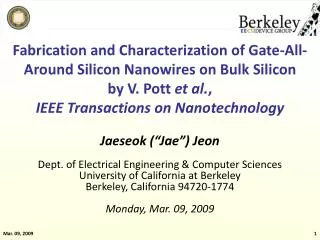
Fabrication and Characterization of Gate-All-Around Silicon Nanowires on Bulk Silicon by V. Pott et al. , IEEE Transactions on Nanotechnology. Jaeseok (“Jae”) Jeon Dept. of Electrical Engineering & Computer Sciences University of California at Berkeley Berkeley, California 94720-1774

E N D
Fabrication and Characterization of Gate-All-Around Silicon Nanowires on Bulk Siliconby V. Pott et al., IEEE Transactions on Nanotechnology Jaeseok (“Jae”) Jeon Dept. of Electrical Engineering & Computer Sciences University of California at Berkeley Berkeley, California 94720-1774 Monday, Mar. 09, 2009
Motivation • Si-nanowire-based gate-all-around (GAA) MOSFETs via top-down approach • Typically, Si-nanowires grown using bottom-up processing • Why top-down processing? » CMOS-compatible » Readily-available resources; has been be dominant technology in semiconductor industry
Top-Down Technique: Process Flow • LPCVD Si3N4 deposition on top of thermal SiO2 • Si-pillar definition • LPCVD Si3N4 deposition • Isotropic etching • Sacrificial oxide growth A-A’ B-B’ For devices with triangular Si-nanowire gates,
Top-Down Technique: Process Flow (Continued) • Si3N4/SiO2 hard-mask stripping • LTO deposition, followed by CMP • Partial LTO etching • Gate oxidation • In-situ doped LPCVD Poly-Si • Poly-Si definition • Implantation and annealing • LTO deposition • Contact opening • Contact metal deposition, definition and FGA A-A’ B-B’
Top-Down Technique:Limitations • Scalability of channel (nanowire) length » Physically limited by lithographic resolution » Sacrificial oxide formed after isotropic etching; channel (nanowire) length increased • Scalability of gate oxide thickness » Thinner gate oxide to drive higher on-current » Thickness non-uniformity; crystalline-orientation-dependent oxidation rate Si-nanowire encapsulated in Poly-Si
Top-Down Technique:Limitations (Continued) • Corner effect » Thin oxide grown at corners; reliability issue under high electrical fields • Reproducibility » Weff down to 16 nm by additional sacrificial oxide formations » Sacrificial oxide formed after isotropic etching » Size and shape: dependent upon timed-etch and oxidation time
Top-Down Technique:Prospects • In contrast to bottom-up approach, » No need to use any catalyst to initiate growth » Process-controlled doping levels and Si crystal orientation » Localized by lithography and etching » Parallel process → higher throughput » CMOS-compatible » Well-defined ohmic contacts connecting nanowires » Higher yield
Top-Down Technique:Prospects (Continued) • Bottom-up approach required for emerging technologies, such as nanotubes and organic semiconductors » Higher density » Allows smaller geometries to be defined; self-assembly → no need for litho » More economical in some sense; c.f. waste of materials during etching » Expected to be more prevalent in semiconductor manufacturing • Combination of top-down and bottom-up approaches Silane-grown Si- nanowires using Au catalyst (T=500°C and P=0.8Torr, from J. Albuschies et al., Microelectronic Engineering, Vol. 83, 2006.) http://www.imec.be/wwwinter/business/nanotechnology.pdf