Download
1 / 42
1.51k likes | 3.81k Views
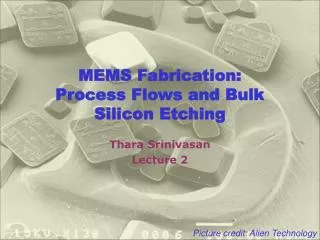
MEMS Fabrication: Process Flows and Bulk Silicon Etching. Thara Srinivasan Lecture 2. Picture credit: Alien Technology. Lecture Outline. Reading Reader: Kovacs, pp. 1536-43, Williams, pp. 256-60. Senturia, Chapter 2. Today’s Lecture Tools Needed for MEMS Fabrication

E N D
MEMS Fabrication: Process Flows and Bulk Silicon Etching Thara Srinivasan Lecture 2 Picture credit: Alien Technology
Lecture Outline • Reading • Reader: Kovacs, pp. 1536-43, Williams, pp. 256-60. • Senturia, Chapter 2. • Today’s Lecture • Tools Needed for MEMS Fabrication • Photolithography Review • Crystal Structure of Silicon • Silicon Etching Techniques
IC Processing Cross-section Masks Cross-section Masks N-type metal oxide semiconductor (NMOS) process flow Jaeger
deposit etch pattern CMOS Processing • Processing steps • Oxidation • Photolithography • Etching • Diffusion • Evaporation and Sputtering • Chemical Vapor Deposition • Ion Implantation • Epitaxy Jaeger Complementary Metal-Oxide-Semiconductor
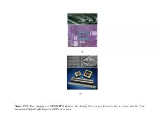
Integrated accelerometer chipFord Microelectronics Micromachined turbine Schmidt group, MIT Angular rate sensor Delphi-Delco Electronic Systems MEMS Devices Microoptomechanical switches, Lucent
Polysilicon level 1 Plate Polysilicon level 2 Polysilicon level 2 Staple Polysilicon level 1 Silicon substrate Hinge staple Silicon substrate Support arm MEMS Devices
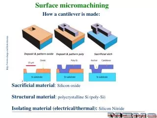
MEMS Processing • Unique to MEMS fabrication • Sacrificial etching • Thicker films and deep etching • Mechanical properties critical • Etching into substrate • 3-D assembly • Wafer-bonding • Molding • Unique to MEMS packaging and testing • Delicate mechanical structures • Packaging: before or after dicing? • Sealing in gas environments • Interconnect - electrical, mechanical, fluidic • Testing – electrical, mechanical, fluidic sacrificial layer structural layer Package Dice Release
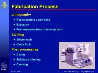
Photolithography: Masks and Photoresist • Photolithography steps • Photoresist spinnning, 1-10 µm spin coating • Optical exposure through a photomask • Developing to dissolve exposed resist • Photomasks • Layout generated from CAD file • Chrome or emulsion on glass • 1-3 $k light-field dark-field
Photoresist Application • Spin-casting photoresist • Polymer resin, sensitizer, carrier solvent • Positive and negative photoresist • Thickness depends on • Concentration • Viscosity • Spin speed • Spin time www.brewerscience.com
Photolithography Tools • Contact or proximity • Resolution: Contact - 1-2 µm, Proximity - 5 µm • Depth of focus • Projection • Resolution - 0.5 (/NA) ~ 1 µm • Depth of focus ~ Fewµms
Materials for MEMS • Substrates • Silicon • Glass • Quartz • Thin Films • Polysilicon • Silicon Dioxide, Silicon Nitride • Metals • Polymers Silicon crystal structure l = 5.43 Å Wolf and Tauber
Silicon Crystallography z z z [001] (110) • Miller Indices (hkl) • Normal to plane • Reciprocal of plane intercepts with axes • (unique), {family} • Direction • Move one endpoint to origin • [unique], <family> y y y [010] (100) (110) (111) x x x [100] {111}
0 1/2 0 1/4 3/4 1/2 1/2 0 1/4 3/4 0 0 1/2 Silicon Crystallography • Angles between planes, • between [abc] and [xyz] is given by: ax+by+cz = |(a,b,c)|*|(x,y,z)|*cos() • {100} and {110} – 45° • {100} and {111} – 54.74° • {110} and {111} – 35.26, 90 and 144.74°
[110] [011] [101] [110] [011] [101] [001] [001] [100] [100] [010] [010] Silicon Crystal Origami {110} (101) {111} {111} (111) (111) {100} (100) • Silicon fold-up cube • Adapted from Profs. Kris Pister and Jack Judy • Print onto transparency • Assemble inside out • Visualize crystal plane orientations, intersections, and directions {110} (101) {111} {111} (111) (111) {100} (001) {110} (101) {110} (011) {110} (011) {111} {111} (111) (111) {100} (100) {100} (010) {100} (010) {110} (110) {110} (110) {110} (110) {110} (110) {110} (101) {110} (011) {110} (011) {111} {111} (111) (111) {100} (001)
Silicon Wafers • Location of primary and secondary flats shows • Crystal orientation • Doping, n- or p-type Maluf
Properties of Silicon • Crystalline silicon is a hard and brittle material that deforms elastically until it reaches its yield strength, at which point it breaks. • Tensile yield strength = 7 GPa (~1500 lb suspended from 1 mm²) • Young’s Modulus near that of stainless steel • {100} = 130 GPa; {110} = 169 GPa; {111} = 188 GPa • Mechanical properties uniform, no intrinsic stress • Good thermal conductor • Mechanical integrity up to 500°C
adsorption desorption surface reaction slowest step controls rate of reaction Bulk Etching of Silicon • Etching modes • Isotropic vs. anisotropic • Reaction-limited • Etch rate dependent on temperature • Diffusion-limited • Etch rate dependent on mixing • Also dependent on layout and geometry, “loading” • Choosing a method • Desired shapes • Layout and uniformity • Surface roughness • Process compatibility • Safety, cost, availability Maluf
Wet Etch Variations • Etch rate variation due to wet etch set-up • Loss of reactive species • Evaporation of liquids • Poor mixing (etch product blocks diffusion of reactants) • Contamination • Applied potential • Illumination
Anisotropic Etching of Silicon • Etching of Si with KOH Si + 2OH- Si(OH)22+ + 4e- 4H2O + 4e- 4(OH)- + 2H2 • Crystal orientation relative etch rates • {110}:{100}:{111} = 600:400:1 • {111} plane has three backbonds below the surface • Energy explanation • {111} may form protective oxide quickly <100> Maluf
KOH Etch Conditions • 1 KOH : 2 H2O (wt.), stirred bath @ 80°C • Si (100) 1.4 µm/min • Etch masks • Si3N4 0 • SiO2 1-10 nm/min • Photoresist, Al ~ fast • “Micromasking” by H2 bubbles leads to roughness • Stirring displaces bubbles • Oxidizer, surfactant additives Maluf
Undercutting • Convex corners bounded by {111} planes are attacked Maluf Ristic
Undercutting • Convex corners bounded by {111} planes are attacked
Corner Compensation • Protect corners with “compensation” areas in layout, Buser et al. (1986) • Mesa array for self-assembly test structures, Smith and coworkers (1995) Alien Technology Hadley Chang
Corner Compensation • Self-assembly microparts, Alien Technology
Other Anisotropic Etchants • TMAH, Tetramethyl ammonium hydroxide, 10-40 wt.% (90°C) • Al safe, IC compatible • Etch rate (100) = 0.5-1.5 µm/min • Etch ratio (100)/(111) = 10-35 • Etch masks: SiO2 , Si3N4 ~ 0.05-0.25 nm/min • Boron doped etch stop, up to 40 slower • EDP (115°C) • Carcinogenic, corrosive • Al may be etched • Etch rate (100) = 0.75 µm/min • R(100) > R(110) > R(111) • Etch ratio (100)/(111) = 35 • Etch masks: SiO2 ~ 0.2 nm/min, Si3N4 ~ 0.1 nm/min • Boron doped etch stop, 50 slower
Boron-Doped Etch Stop • Control etch depth precisely with boron doping (p++) • [B] > 1020 cm-3 reduces KOH etch rate by 20-100 • Gaseous or solid boron diffusion • At high dopant level, injected electrons recombine with holes in valence band and are unavailable for reactions to give OH- • Results • Beams, suspended films • 1-20 µm layers possible • p++ not compatible with CMOS • Buried p++ compatible
Microneedles Ken Wise group, University of Michigan
Microneedles Wise group, University of Michigan
Microneedles Ken Wise group, University of Michigan
Electrochemical Etch Stop • Electrochemical etch stop • n-type epitaxial layer grown on p-type wafer forms p-n diode • p > n electrical conduction • p < n “reverse bias” • passivation potential – potential at which thin SiO2 layer forms • Set-up • p-n diode in reverse bias • p-substrate floating etched • n-layer above passivation potential not etched Maluf
Electrochemical Etch Stop • Electrochemical etching on preprocessed CMOS wafers • N-type Si well with circuits suspended from SiO2 support beam • Thermally and electrically isolated • TMAH etchant, Al bond pads safe Reay et al. (1994)
Deposit insulator (100) Si diaphragm P-type diffused piezoresistor Bondpad Metal conductors Diffuse piezoresistors n-type epitaxial layer R1 R2 R1 R3 R3 (111) (111) Deposit & pattern metal Electrochemical etch of backside cavity Backside port Anodically bonded Pyrex substrate Etched cavity Anodic bonding of glass Pressure Sensors • Bulk micromachined pressure sensors • In response to pressure load on thin Si film, piezoresistive elements detect stress • Piezoresistivity – change in electrical resistance due to mechanical stress • Membrane deflection < 1 µm p-type substrate & frame Maluf Integrated Pressure Sensor, Bosch
HNA: hydrofluoric acid (HF), nitric acid (HNO3) and acetic (CH3COOH) or water HNO3 oxidizes Si to SiO2 HF converts SiO2 to soluble H2SiF6 Acetic prevents dissociation of HNO3 Etch masks SiO2 etched at 300-800 /min Nonetching Au or Si3N4 Isotropic Etching of Silicon pure HF reaction-limited pure HNO3 diffusion-limited Robbins
Pro and Con Easy to mold from rounded channels Etch rate and profile are highly agitation sensitive Isotropic Etching Examples Tjerkstra, 1997 • 5% (49%) HF : 80% (69%) HNO3 : 15% H2O (by volume) • Half-circular channels for chromatography • Etch rate 0.8-1 µm/min • Surface roughness 3 nm
Dry Etching of Silicon • Dry etching • Plasma phase • Vapor phase • Plasma set-up and parameters • RF power • Pressure • Nonvolatile etch species • Plasma phase etching processes • Plasma etching • Reactive ion etching (RIE) • Inductively-coupled plasma RIE
Plasma Etching of Silicon • SF6 • Plasma phase • Vapor phase
High-Aspect-Ratio Plasma Etching • Deep reactive ion etching (DRIE) • Inductively-coupled plasma • Bosch method for anisotropic etching, 1.5 - 4 µm/min • Etch cycle (5-15 s) SF6 (SFx+) etches Si • Deposition cycle (5-12 s) C4F8 deposits fluorocarbon protective polymer (-CF2-)n • Etch mask selectivity: SiO2 ~ 200:1, photoresist ~ 100:1 • Sidewall roughness: scalloping < 50 nm • Sidewall angle: 90 ± 2° Maluf
DRIE Issues • Etch rate is diffusion-limited and drops for narrow trenches • Adjust mask layout to eliminate large disparities • Adjust process parameters (etch rate slows to < 1 µm/min) • Etch depth precision • Etch stop ~ buried layer of SiO2 • Lateral undercut at Si/SiO2 interface ~ “footing” Fig 3.15 p.68 Maluf Maluf
Comb-drive Actuator DRIE Examples Keller, MEMSPI
Vapor Phase Etching of Silicon • Vapor-phase etchant XeF2 2XeF2(v) + Si(s) 2Xe(v) + SiF2(v) • Etch rates: 1-3 µm/min (up to 40) • Etch masks: photoresist, SiO2, Si3N4, Al, metals • Set-up • Closed chamber, 1 torr • Pulsed to control exothermic heat of reaction • Issues • Etched surfaces have granular structure, 10 µm roughness • Hazard: XeF2 reacts with H2O in air to form Xe and HF Xactix
Etching with Xenon Difluoride • Example Pister group
Laser-Driven Etching • Laser-Assisted Chemical Etching • Mechanism • Etch rate: 100,000 µm3/s; 3 min to etch 500500125 µm3 trench • Surface roughness: 30 nm RMS • Serial process: patterned directly from CAD file . • Laser-assisted etching of A 500500 µm2 terraced silicon well. Each step is 6 µm deep. Revise, Inc.