Download
1 / 6
70 likes | 107 Views
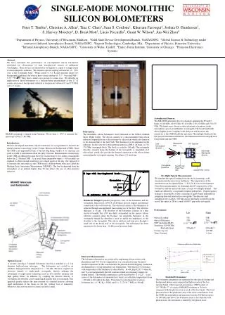
Explore the fabrication of single crystal silicon nanosurfaces with controlled separation for parallel plate capacitor electrodes. The process involves fracturing silicon to create nanosurface pairs and structures to control their separation. Experimental stages include specimen orientation, thickness, and notching variations. Predicted capacitor performance includes native oxide thickness of 4 nm, stable gap of 4 nm, and operational voltage at 1V. The development timeline features a composite micrograph of the process device in ambient air.

E N D
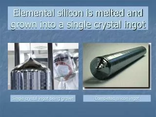
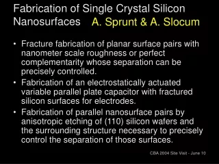
Fabrication of Single Crystal Silicon Nanosurfaces A. Sprunt & A. Slocum • Fracture fabrication of planar surface pairs with nanometer scale roughness or perfect complementarity whose separation can be precisely controlled. • Fabrication of an electrostatically actuated variable parallel plate capacitor with fractured silicon surfaces for electrodes. • Fabrication of parallel nanosurface pairs by anisotropic etching of (110) silicon wafers and the surrounding structure necessary to precisely control the separation of those surfaces.
Two-Stage Device Experimented with different specimen orientations, specimen thicknesses, and notching techniques.
Predicted Performance & Fabrication • Native oxide thickness: 4 nm • Minimum stable gap: 4 nm • Capacitor Voltage: 1 V Native Oxide Thickness Composite micrograph of process development device released in air.