Download
1 / 20
210 likes | 349 Views
Electrical Characterization of Nanowires. Steven Kuo San Jose State University Thesis Advisor Dr. Emily Allen San Jose State University. Research Advisor Dr. Geetha R. Dholakia NASA AMES Center for Nanotechnology. Task.

E N D
Electrical Characterization of Nanowires Steven Kuo San Jose State University Thesis Advisor Dr. Emily Allen San Jose State University Research Advisor Dr. Geetha R. Dholakia NASA AMES Center for Nanotechnology
Task • Synthesisof nanowires by templated sol-gel growth and structural and electronic studies for applications in spin-based devices.
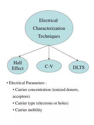
Outline • Background • Research Tasks • Methods • Results • Summary of Work
Why Nanotechnology? • Limit in today’s electronic device process • Need alternate method to continue shrinking • Nanowires - key group of nanoscale materials in developing devices • Nanoelectronics benefit from knowledge of material characteristics
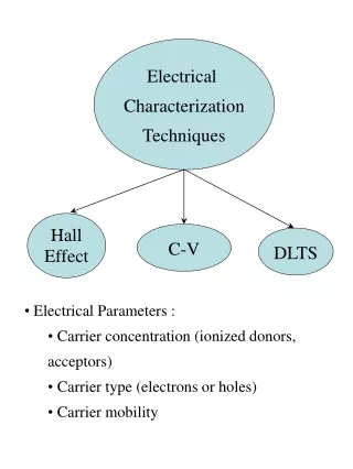
Why do we need to characterize nanowires? • Bulk properties differ from nanoscale properties • Surface and grain boundary scattering • Need a method of electrical character… nanoscale materials in order to produce useful devices
Electrical properties need to be studied…but how? Current method of electrical characterization Wire diameter is microns wide What happens when… Wire diameter is only nanometers wide?
Research Tasks • Task 1: Separation and alignment of nanowires • Removal of nanowires from • Quick and easy manipulation of nanowires onto contact pads of devices • Task 2: Setup IV Measurement System • MMR Technologies Cryocooler • LabVIEW Instrument interface • Task 3: IV Measurements • Determine electrical characteristics of nanowires by a 4 probe method • Resistivity measurements across temperature range of 80K – 400K • Determine band gap information for semiconducting nanowires
Research Steps • Part 1: Liberate nanowires from anodized alumina template (completed) • Part 2: Align nanowires using electric field (completed) • Part 3: Setup temperature dependent measurement system (completed) • Part 4: Band gap measurements on single nanowire
ln σ -Eg/2k 1/T Band gap information can be determined • From 4 probe measurements • Resistivity can be determined • From the relationship ρ=1/σ • Conductivity can be determined • Plot ln σ vs. 1/T • Using the equation where x is 1/T • Eg is the band gap of the material
Electric field Nanowire where Electrodes How do we manipulate nanowires when they are so small? • Dielectrophoresis • Force which acts on any polarizable object in a nonuniform electric field
E-Field Modeling • Simulation of the expected e-field was calculated using Maxwell software • E-Field expected to be strongest at corners between the electrodes
E-Field Alignment Device Design and Fabrication • Interdigitated electrodes fabricated at Microelectronics Process Engineering Lab at SJSU • Interdigitated electrodes 3-6 um spacings • 200nm Al on 700nm SiO2 insulating layer • 4 in. wafer with approx. 33 devices
Finished Electrode Devices Optical images of finished wafer and single device SEM images of fabricated devices
Anodized Alumina Template TiO2 Nanowires Nanowire removal from template • AAT removed with NaOH • Nanowires released by sonication • BIG Problem!!
E-Field Alignment of Nanowires on Devices • TiO2 nanowires are aligned across 3 – 6 um spaced electrodes by an AC bias • 25Hz – 30MHz • 10 Vpp
Temperature Dependent Resistivity Measurements • MMR Technologies Cryocooler 80K – 400K temperature range • Verified to 80K • Keithley Electrometer and Current Source • LabVIEW interface to control electrometer and current source
Ongoing Work • Redesign of the test device for accommodation in the MMR cryocooler Possible new electrode design (not to scale)
Summary of Work to Date • Nanowire alignment on electrodes has been achieved • Temperature dependent resistivity measurement system completed • Publications • Steven Kuo, Geetha R Dholakia and E. L. Allen, “Self assembly of TiO2 nanowires onto devices by dielectrophoresis,” accepted for poster presentation Spring Materials Research Society Meeting, San Francisco (March 2007). • Geetha R Dholakia , Steven Kuo and E. L. Allen “Self assembly of organic nanostructures and dielectrophoretic assembly of inorganic nanowires,” accepted for presentation at American Physical Society Conference, April 2007.
Work to be Completed by Aug 07 • Task 3: • New mask • devices
Acknowledgements • DMEA Grant H94003-06-2-0605 • Ms. Rebka Endale, SJSU • Dr. Ann Marshall, Stanford Nanocharacterization Lab • Mr. Neil Peters, Microelectronics Process Engineering Lab • Ms. Anastasia Micheals, SEM Lab