Download
1 / 9
90 likes | 230 Views
Bent Weber 1 , S. Mahapatra 1,2 , W, Clarke 1 , M. Y. Simmons 1,2 1) School of Physics, The University of New South Wales, Sydney, NSW 2052, Australia 2) Australian Research Counsel Centre of Excellence for Quantum Computer Technology, Sydney, Australia H. Ryu , S. Lee, G. Klimeck

E N D
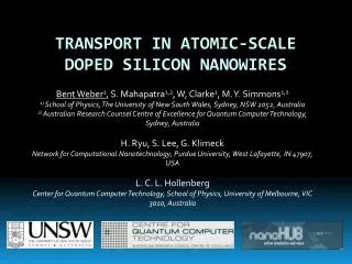
Bent Weber1, S. Mahapatra1,2, W, Clarke1, M. Y. Simmons1,2 1) School of Physics, The University of New South Wales, Sydney, NSW 2052, Australia 2) Australian Research Counsel Centre of Excellence for Quantum Computer Technology, Sydney, Australia H. Ryu, S. Lee, G. Klimeck Network for Computational Nanotechnology, Purdue University, West Lafayette, IN 47907, USA L. C. L. Hollenberg Center for Quantum Computer Technology, School of Physics, University of Melbourne, VIC 3010, Australia Transport in atomic-scale doped silicon nanowires
Applications of Silicon Nanowires In-plane gates / leads for silicon donor-based quantum computing Silicon nanowire transistors Fuechsleet al., Nat. Nanotech., advance online publication (2010) poly gate oxide Cui et al., NanoLetters3 (2), 149 (2003) SiNW 5 nm Singh et al., IEEE Electron Device Letters 27 (5), 383 (2006) Fuhrer et al., NanoLetters9 (2), 707 (2009)
Limits of Conduction in Nanowires ≥ 30 nm As the diameter reaches the nano-scale: • Surface scattering (< 4 nm) • Carrier depletion due to surface/interface states • Doping challenging • Limited to (~ 1020 cm-3) (VLS) • Dopant-segregation (< 5 nm) • Quantum confinement (<10 nm) • Dielectric confinement (<30 nm) Electron beam lithography, RIE etching Vauretteet al., J. Vac. Sci. Technol. B 26 (3), 945 (2008) 3 nm Vapor-liquid-solid (VLS) growth 2 nm 1.7 nm Wu et al., NanoLetters4 (3), 433 (2004) • STM-fabricated wires: • Elimination of surface effects • High doping levels (~ 1021 cm-3) • Full dopant activation 25 nm STM-lithography, δ-doping and molecular beam epitaxy
Atomic-Precision Doping by STM Hydrogen-terminated Si(001)-2x1 surface DV 4 nm STM-tip H2 STM-patterned SDB STM hydrogen lithography 4 nm H:Si PH3 PH SDB PH3 dosing 4 nm p(2x2)-PH2 V1 ejected Si Dopant incorporation (~350°C) ¼ ML density D 4 nm DB S Si Al contacts 5 μm ~25nm epitaxial encapsulation (~250°C) V2 UHV
Ohmic Conductors at the Atomic Scale S4 90 nm 27 nm 50 nm Ruesset al. Nanotechnology 18, 044023 (2007) 200 nm 200 nm 300 nm RD = 5.3 kΩ RD = 10.1 kΩ RD = 17.1 kΩ RD = 82.3 kΩ 30 nm S S1 S3 S2 1.7 nm 4.6 nm 2.3 nm 2.3 nm D T = 4.2 K
Atomistic Modeling of Si Nanowires Electronic structure modeling with atomistic representation, using NEMO-3D dleff=3.4 nm dlith=1.7 nm Phosphorus Silicon Aeff ¼ ML planar coverage ND,2D = 2.4 x 1014 cm-2 d < 1 nm ND,3D = ~ 1021 cm-3 >> NMott ~ 3 x 1018 cm-3 T = 4K Direction of transport
Diameter-Independent Resistivity Yamada et al., Jap. J. Appl. Phys. 28 (12), L2284 (1989) bulk resistivity (T= 4 K) ≥ 6 nm Bjorket al., Nat. Nanotech., 4 (2), 103 (2009) 9x10¹⁸ 3x10¹⁹ 1.5x10²⁰ Diarraet al., Phys. Rev. B 75 (4), 045301 (2007)
Conclusions • Narrowest doped silicon nanowires, showing Ohmic conduction • Diameter-independent resistivity, comparable to bulk value • full dopant activation down to ~2 nm • Atomistic tight-binding calculations (NEMO-3D) to compute electronic structure T = 4K
Thanks to … • Dr. A. Fuhrer (now IBM Rueschlikon, Switzerland) and Dr. T.C.G. Reusch (now OSRAM Opto Semiconductors, Regensburg, Germany) • The UNSW Quantum Electronic Devices group of Prof. A. R . Hamilton (especially Dr. T. Martin, Dr. O. Klochan, A/Prof A. P. Micolich) • This work was supported by the Australian Research Council, the Army Research Office under contract number W911NF-08-1-0527 and the National Science Foundation (NSF). Computational resources on nanoHUB.org, NICS, TACC, and Oak Ridge National Lab were utilized.