TTL Logic: Transistors and Chip Improvement
430 likes | 451 Views
Explore how TTL logic utilizing only transistors and resistors improves fan-out compared to earlier RTL and DTL logic families. Learn the calculations for VTC and see why TTL gates are advantageous over DTL for faster switching speeds.

TTL Logic: Transistors and Chip Improvement
E N D
Presentation Transcript
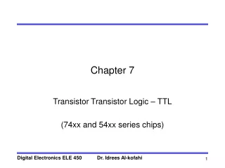
Chapter 7 Transistor Transistor Logic – TTL (74xx and 54xx series chips)
Transistor Transistor Logic • DTL was able to improve fan-out compared to RTL. However, that was done at the expense of: • Transient response. • Chip area. • A solution for the problem was proposed in the form of a new logic family which utilizes only transistors and resistors. • BJTs are smaller than diodes.
V CC R R C B V out V Q in Q o I Basic TTL Inverter
V CC R R C V B CC V R out R C B V Q in Q o I V V out in Q o D D I L TTL vs. DTL • If we compare the basic DTL and TTL gates, we find that the input and level-shifting diodes of DTL can be combined into the input BJT of TTL. • The advantage is that the BJT requires less silicon area and the propagation delay is improved by a factor of 10.
Calculating the VTC • VOH: • For Vin very low, the base-emitter junction of QI will be forward biased. • The base-collector junction will also be forward biased. • Therefore, QI will be saturated. • The base-emitter voltage of QO is: VBE,O = VCE,I(Sat) + Vin • Therefore, QO will be cut-off • Therefore, Vout = VOH = VCC
Calculating the VTC (Contd.) • VIL: • As Vin is increased, VB of QO will also increase. Eventually, QO will turn on. • This happens when: Vin = VIL = VBE,O (FA) – VCE,I (Sat) • VOL: • As Vin is increased even more, QO comes closer to Saturation and eventually saturates. • At that point: Vout = VOL = VCE,O (Sat)
V out V = V OH CC V = V (Sat) OL CE VIn VIL = VBE,O (FA) – VCE,I (Sat) VIH = VBE,O (Sat) – VCE,I (Sat) Calculating the VTC (Contd.) • VIH: • The point where QO is just saturating: Vin = VIH = VBE,O (Sat) – VCE,I (Sat)
What about the currents? • If we look at the currents in the circuit, we find that QI and QO cannot both remain saturated at the same time. • If QI is saturated, a positive IC,I must flow into the collector of QI. • IF QO is saturated, a positive IB,O must flow into the base of QO. • Impossible!!!! • If we look at the voltages, we find that right after QO saturates, the base-emitter junction of QI will become reverse biased while the base-collector junction is still forward biased. • Therefore, QI will turn into Reverse Active mode. • Under reverse active mode, IC,I flows out of the collector of QI. • This current will flow into the base of QO maintaining it in saturation.
VCC RC RB Vout Vin > VIH IB,O QI QO Sat Sat IC,I The Currents • If both QI and QO are saturated, then both IC,I and IB,O need to be positive. • Impossible!!
The Voltages VIH = VBE,O (Sat) – VCE,I (Sat) = ~0.6 V V CC R R C B Vout VBE,I < ~ 0.8 VBC,I (FB) ~ 0.6 Vin > VIH > ~0.6 V QO Sat QI QI cannot remain in Saturation VBE,O (Sat) ~ 0.8 VB,I = ~1.4 V
The VTC Vout QO Cutoff QI Sat VOH = VCC QO F. A. QI Sat QO Sat QI Sat QO Sat QI R. A. VOL = VCE,O (Sat) VIn VIL = VBE,O (FA) – VCE,I (Sat) VIH = VBE,O (Sat) – VCE,I (Sat)
V CC R R C B V out V in Q o D D I L R D Do we need a pull-down resistor? • For DTL, a pull-down resistor was added to quickly discharge the charge built into the base of the saturated QO when it is switching to cut-off. • When QO is saturated, there is about 0.8 V worth of charge built up in the base. • When QO turns off, this charge will flow primarily through RD down to ground. • The current through RDwill be: (using typical values)
VCC RB RC Vouy Vin QO QI What about TTL? • When Vin is switched from high to low, QO is still in saturation. • So, VC,I = VBE,O (Sat) • VE,I is connected to the output of a previous TTL gate. • VE,I = VOL = VCE,O’ (Sat) • The base emitter voltage of QI will be VBE (FA) • Therefore, • VB,I = VCE,O’ (Sat) + VBE,I (FA) • VBC,I = VCE,O’ (Sat) + VBE,I (FA) – VBE,O (Sat) • This is not enough to saturate QI. Therefore, it operates in FA mode. • The resulting collector current is IC,I = bf IB,I • Using typical values, IC,I = 102.5 mA • Comparing to DTL, the TTL current is 600 times larger. • So, a TTL gate can switch 600 times faster than DTL without a pull-down resistor.
V CC V V CC CC R R C B R R R R V C C B B V out A Q o V V D D out out V VA A L A Q Q V o o B VB VC D V B B V C D V C C The TTL NAND Gate • For DTL, a NAND gate was built as shown below on the left. • The same thing can be implemented in TTL by combining the input diodes and the level shifting diode into multiple transistors. • Or, the input transistors can be combined into a “multi-emitter” BJT as shown in the figure on the right.
E3 E2 E1 B C B E3 E2 E1 C The Multi-Emitter BJT • All three emitters share the same base and collector. • The only difference is that instead of having one IE, we now have IE. • So, for a multi-emitter BJT, the basic current relationship becomes: IE = IE1 + IE2 + IE3 = IC + IB Circuit Symbol Physical Structure
V CC R R C B V out VA Q o VB VC The TTL NAND Operation • If any input is low: • The corresponding B-E junction will be forward biased. • This allows a large base current to flow in RB and makesQI saturate. • QO will turn off and the output will be high. • If all inputs are high: • All B-E junctions are reverse biased. • The B-C junction is forward biased. • QI will operate in reverse active mode. • A large current will flow into the base of QO sending it into saturation. • The output voltage will be low.
VCC RCP RC RB QP VA QS QI DL VB Vout DCA DCB QO RD TTL with Totem-Pole Output
TTL with Totem-Pole Output (Contd.) • The combination of RCP and QP provide active pull-up. • This increases the amount of sourcing current available for turning the load gates on when the output is changing from low to high. • QS acts as an emitter follower increasing the amount of current going into the base of QO ensuring that it will saturate. • It also provides logic inversion to make sure that QP and QO are not on at the same time. • Diode DL is also used to ensure that the transistors do not operate at the same time.
VCC RCP RC RB QP VA QS DL VB Vout DCA DCB QO RD The VTC of the Basic TTL Gate • VOH: • For a low Vin, IB,I will be large. • However, IC,I will only be the leakage current flowing out of the base of QS. • Therefore, IC,I << IB,I and QI is saturated. • The voltage at the base of QS is VB,S = Vin + VCE,I (Sat) • This is not enough to turn QS on, QS is cut-off. • IE,S = 0 IB,O = 0 QO is also cut-off. • VB,P = VCC • Therefore, Vout = VOH = VCC – VBE,P (FA) – VD,L (ON) FA VB,P IB,I QI VB,S ON IC,I Sat off IE,S IB,O off
VCC RCP RC RB QP VA QS DL VB Vout DCA DCB QO RD The VTC of the Basic TTL Gate • VIL: • As Vin is increased, so will VB,S. • This will continue until VBE,S = VBE (FA). • At that point QS will be at Edge Of Conduction. • Vin at this point is: VIL = VBE,S (FA) – VCE,I (Sat) FA QI VB,S Sat ON E. O. C IE,S IB,O off
VCC RCP RC RB QP VA QS DL VB Vout DCA DCB QO RD The VTC of the Basic TTL Gate • VIB: • As Vin is increased even more, QS goes into forward active mode. • IE,S is no longer 0. But IB,O is still 0. • The current will go through RD.This creates a voltage difference across RD. • As Vin rises, so will the voltage across RD. • Eventually, this will be enough to put QOat edge of conduction. • The input voltage needed for that is: VIB = VBE,O (FA) + VBE,S (FA) – VCE,I (Sat) • What about QP and DL? • As IE,S 0, IC,S cannot be 0. • Most of IRC will go to IC,S and IB,P willapproach 0. • Therefore, QP and DL will start to go into cutoff mode. IRC IB,P Off IC,S QI Sat Off FA IE,S IB,O E. O. C IRD
VCC RCP RC RB QP Off VA QS DL QI VB VB,S Sat Off Vout FA IE,S DCA DCB QO IB,O RD E. O. C IRD The VTC of the Basic TTL Gate • VOB: • At that point, Vout = VCC – IRC * RC – VBE,O (FA) – VD,L (ON) Therefore,
VCC RCP RC RB QP VA QS DL VB Vout DCA DCB QO RD The VTC of the Basic TTL Gate • VIH: • As Vin is increases still more, QS and QO will both saturate. • The input voltage needed for that is: VIH = VBE,O (Sat) + VBE,S (Sat) – VCE,I (Sat) • VOL: • At that point: Vout = VOL = VCE,O (Sat) FA VB,P QI VB,S Sat ON FA IE,S IB,O E. O. C IRD
Will QI Switch to Reverse Active? • Yes. • For QI to switch to reverse active, we need • VBE,I < 0.7 • For Vin > VIH • VB,I = VBC,I (FB) + VBE,S (Sat) + VBE,O (Sat) • For typical values, VB,I = 0.6 + 0.8 +0.8 = 2.2 V • Therefore, QI will switch to RA mode whenVin > 1.5 V
Example • Calculate the VTC using typical values: • VOH = VCC – VBE,P (FA) – VD,L (ON) = 5 – 0.7 – 0.7 = 3.6 V • VIL = VBE,S (FA) – VCE,I (Sat) = 0.7 – 0.2 = 0.5 V • VIB = VBE,O (FA) + VBE,S (FA) – VCE,I (Sat) = 0.7 + 0.7 – 0.2 = 1.2 V • VOL = VCE,O (Sat) = 0.2 V • VIH = VBE,O (Sat) + VBE,S (Sat) – VCE,I (Sat) = 0.8 + 0.8 – 0.2 = 1.4 V
1 2 VOH = 3.6 V VOB = 2.5 V 3 4 5 VOL = 0.2 V VIH = 1.4 V VIB = 1.2 V VIL = 0.5 V The VTC
TTL Fan-out VCC VCC R’CP VCC RCP RC RB Q’P RC RB QP D’L QS QI DL QS QI Q’O DCA QO DCA RD RD
IIL • The low input comes from the saturated Q’O of a previous similar gate. • Therefore, Vin = VCE,O’ (Sat) • QI will be saturated • VB,S will beVCE (Sat) + VCE (Sat) • QS is off. • IIL = IE,I • IE,I = IC,I + IB,I • IC,I = 0. VCC VCC R’CP RC RB IB,I Q’P D’L VB,S QS QI IC,I Sat Off IIL Sat Q’O DCA RD
VCC RCP RC RB QP QS QI DL Off DCA QO Off Sat RA IOL RD Sat IOL • The low output comes from QO being saturated and both QP and DL being off. • IOL = IC,O • IC,O = sbFIB,O • Max fan-out, when s = 1 • IB,O = IE,S – IRD • IE,S = IC,S + IB,S • IB,S = IC,I • QI is R.A., therefore, • IC,I = (1 + bR) IB,I
Example • Calculate output-low fan-out using typical values. IB,S = IC,I = (1 + 0.1) .675 m = .743 mA IE,S = .743 m + 2.5 m = 3.243 mA IB,O = 3.24 m – 0.8 m = 2.44 mA IOL = IC,O = 1 X 25 X 2.44 m = 61 mA
VCC VCC R’CP FA RCP RC RB IB,I Q’P ON QP VB,I D’L QS QI DL Sat IIH RA Q’O DCA QO Sat RD IIH • The high input comes from QP and DL of the driving gate both being on. • This makes QI RA, and QS and QO both saturated. • We can determine VB,I = VBE,O (Sat) + VBE,S (Sat) + VBC,I (RA) • Since QI is RA, • IIH = IE,I = bR IB,I
VCC RCP RC FA RB QP ON QS VB,I DL OFF QI IOH RA QO Off IOH • Since the QI’s of the load gates must be kept in RA mode, • Vout > VB,I – VBE,I (FA) • Therefore, • VB,P > VB,I – VBE,I (FA) – VD,L (ON) – VBE,P (FA) • IOH = IE,P = (1 + bF) IB,P
Example • Calculate output-high fan-out using typical values. • VB,I = VBE,O (Sat) + VBE,S (Sat) + VBC,I (RA) = 0.8 + 0.8 + 0.7 = 2.3 V • IIH = IE,I = bR IB,I = 0.1 X 0.675 m = 0.0675 mA • VB,P > VB,I – VBE,I (FA) – VD,L (ON) – VBE,P (FA) • VB,P > 2.3 – 0.7 – 0.7 – 0.7 = 0.2 V • IOH = IE,P = (1 + bF) IB,P = (1 + 25) X 3 m = 78 mA
TTL Power Dissipation • Output Low State: • ICC (OL) = IRCP + IRC + IRB • QP is cut off IRCP = 0. • QS and QO are Sat. • QI is RA, therefore VCC IRCP IRC IRB RCP RC RB Off QP Off QS QI DL Sat RA DCA QO Sat RD
TTL Power Dissipation • Output High State: • ICC (OH) = IRCP + IRC + IRB • If we assume no loads IRCP = 0, IRC = 0. • QI is saturated and this gate is driven by a similar gate, therefore VCC IRCP IRC IRB RCP RC RB FA QP ON QS QI DL Off Sat DCA QO Off RD
Example • Calculate the average power dissipation of the TTL gate using typical values • ICC (OL) = IRC + IRB • ICC (OH) = IRB
Example (Contd.) ICC (OL) = 2.5 m + 0.675 m = 3.175 mA ICC (OH) = 1 mA • Should there be loads connected, ICC (OH) will increase and so will the power dissipation.
Open Collector TTL • If we remove the active pull-up section, we end up with a gate that can be used for connecting to a common bus. • For a low output, QOsaturates and pulls thebus line low. • For a high output,an external pull-upresistor is added tothe bus line. VCC RC RB VA QS QI VB Vout DCA DCB QO RD
Open Collector NAND gates • If any NAND gate produces a low, the whole line is drawn low. • The NAND gates cannot produce a logic high. • They will basically produce a high impedance state. • The pull-up resistor will pull the line up to VCC. VCC
VCC 120 W 1.6 kW 4 kW QP Vin QS QI DL Vout DCA QO 1 kW Typical TTL Values (74xx) • VOH = 3.6 V • VIL = 0.5 V • VOB = 2.5 V • VIB = 1.2 V • VOL = 0.2 V • VIH = 1.4 V • IIL = 1 mA • IOL = 100 mA • Max N = 100 • Ave. PDisp = 10 mW • Propagation Delay = 10 nS • PDP = 100
VCC 500 W 20 kW 40 kW QP Vin QS QI DL Vout DCA QO 12 kW Low Power TTL – LTTL (74Lxx) • To reduce the power, we need to reduce ICC. • The easiest way is to increase the sizes of the resistors. • Ave PDisp = 0.9 mW • The price is a reduction in Fan-out and switching speed. • N = 50
Darlington Pair VCC 58 W 760 W 2.8 kW QP QP2 Vin QS 4 kW QI Vout DCA QO 470 W High Speed TTL – HTTL (74Hxx) • To increase the transition speed, we need to increase the currents. • The easiest way is to reduce the sizes of the resistors. • In addition, a combination known as the Darlington Pair replaces QP to increase the amount of current that can be supplied to the load when the output is switching from low to high. • Of course, the price is increased power dissipation. • Ave. PDisp = 20 mW