Download
1 / 44
470 likes | 659 Views
Scanning Probe Microscopy- Application beyond Imaging Nanofabrication. Dec. 03 2009. There’s Plenty of Room at the Bottom. Richard Feynman, 1959 at California Institute of Technology. The original nanotechnology vision. Consider the possibility that we too can make a thing very small

E N D
Scanning Probe Microscopy- Application beyond Imaging Nanofabrication Dec. 03 2009
There’s Plenty of Room at the Bottom Richard Feynman, 1959 at California Institute of Technology The original nanotechnology vision
Consider the possibility that we too can make a thing very small which does what we want---that we can manufacture objects at that level! Write all 25,000 pages of the 1959 edition of the Encyclopedia Britannica in an area the size of a pin head.
He predicted the using big tools to make smaller tools suitable For making yet smaller tools, and so on, until researchers had Tools sized just right for directly manipulating atoms and molecules Chemistry would become a matter of literally placing atoms one By one in exactly the arrangement you want.
Lithography Procedures in Semiconductor Industry Developing Deposition Liftoff Illuminating with light Under a mask Photoresist Si Wafer
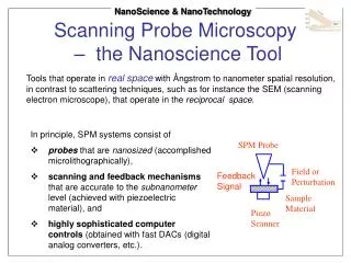
Scanning Probe Microscopy Highly localized “field” Electric field, Magnetic field … Extended eyes Extended hands Probe Manipulator To see atoms, molecules and any nanostructures To characterize local property To move atoms, molecules, locally modify surfaces. To fabricate any anostructures
Positioning single atoms with scanning tunnelling microscope. Eigler, D. M. Nature 1990, 344, 6266 The entire logo ~ 3nm! The scanning tunneling microscope (STM) at low temperature. (4K) to position 35 Xe atoms on a single-crystal Ni surface. THIS IS FUN!!!
Commercial Nanomanipulator NanoManipulator™ DP-100/200 http://www.3rdtech.com/nanods02v2pg12forweba.PDF
The NanoManipulator system uses the industry’s most advanced haptic display device – a SensAble Technologies PHANTOM Desktop – to provide continual force feedback for investigating and manipulating your sample. Unlike the visual display from an SPM, which cannot update during sample manipulation, the haptic display of the NanoManipulator provides continual feedback on the sample’s topography. Scientists can manually change the lateral position of the probe, while the microscope maintains quantitative force control, and have precise knowledge of the location of the sample and the probe throughout. This compensates for the effects of drift and hysteresis, enabling rapid, accurate manipulations that are almost unthinkable otherwise
Nano-Plough The Logo of Peking University indented on an Au-Pd film with a modification force of 20 nN
Nanoclusters can be produced and organized into patterns using the custom-built nanofabricating system based on Scanning probe Microscope. Here shown are gold nanoclusters, ~80nm in diameter, field-evaporated from AFM tip on gold/mica substrates. Nano-Evaporation
Nano-oxidation HF development Nanotrench on Silicon
Heterogeneous Catalysis of a Copper-Coated Atomic Force Microscopy Tip for Direct-Write Click Chemistry Walter F. Paxton, Jason M. Spruell, and J. Fraser Stoddart, J ACS 2009
Dip Pen Lithography NanoDelivery Science 1999, 283, 663 Chad A Mirkin
The resolution of DPN depends on several parameters: • The grain size of the substrate • the texture of paper controls the resolution of conventional writing. • chemisorptions and self assembly can be used to limit the diffusion of • the molecules after deposition. • The tip-substrate contact time and thus the scan speed • influence DPN resolution. • by controlling the rate of ODT transport from the tip to the substrate. • Relative humidity seems to affect the resolution of • the lithographic process • The size of the water meniscus that bridges the tip and substrate • depends on relative humidity
Thiol–Au (organic molecule, thiol functionalized protein, Alkylhiol-modified oligonucleotides) Alkylsilazanes and Inorganic salts – oxidized Si surface Alkylsilazanes – Oxidized GaAs Conducting polymer-- Modified Si surface ( electrostatic)
Electrochemical AFM “ Dip-Pen” Lithography Metal salts, conducting polymer monomer -Si surface ( Au, Pt) JACS 2001, 123, 2105 JACS 2002, 124, 522
Direct Patterning of Modified Oligonucleotides on Metals and Insulators by Dip-Pen Nanolithography Science 2002, 296, 1836
Transfering ODN to insulating substates The surface of a thermally oxidized wafer was activated by treatment with 3’-mercaptopropyltrimethoxysilane (MPTMS). The preparation and inking of the AFM tip were performed exactly as DNA onto gold surfaces, but in this case, oligonucleotides With for the patterning of 5’-terminal acrylamide groups were used. Under the DPN conditions of room temperature and 45% relative humidity, the acrylamide moieties react by Michael addition with the pendant thiol groups of the MPTMS to covalently link the DNA to the surface. After patterning, the substrate was passivated by reaction with buffered acrylic acid monomer at pH 10 (Apogent Discoveries Quench Solution, 30 min.).
Transfering ODN to insulating substates Direct DPN transfer of DNA onto insulating substrates. (A) Epifluorescence micrograph of fluorophore-labeled DNA (Oregon Green 488-X) hybridized to a DPN-generated pattern of complementary oligonucleotides on an SiOx surface. The scale bar represents 12 µm. (B) Tapping-mode AFM image of oligonucleotide-modified gold nanoparticles (13-nm diameter) hybridized to a second, high-resolution pattern after removal (using DI water) of the fluorophore-labeled DNA. The scale bar represents 1.5 µm, and the space between the arrows is 100 nm.
L D scattering Macrowires Classical conductance: L >> electron mean free path D>> lF, electron wavelength I V Conductance G (G0) G changes continuously as D. D
where, N=0, 1, 2, 3, … and G0 = 2e2/h = 12.9k Nanowires Quantum conductance: L < electron mean free path ballistic transport (no collisions). D~ lF, electron wavelength wave nature of electron important. D=lF/2 D=lF Conductance Quantized! D ~ lF ~ 1-3 Å! G (G0) -1 D
lF ~ 1-3 Å – must be atomically thin! l e ~ nm. Room temperature. Conductance Quantization in Metal Nanowires How to fabricate such thin wires?
Atomically thin! stretching Ohnish et al. Fabrication: Mechanical MethodGimzewski et al.,Agrait et al.,Pascual et al… G (G0)
Interactions of Molecules with Metallic Quantum Wires He and Tao, Adv. Mater. 2001, 13, 659
Using STM Principle to Fabrication of Nanogaps for Molecular Electronics A Key Task:How to wire them?- connect a single molecule to external world
Mechanical Method Many nanowires can be quickly produced. Lack of long-term stability Not device compatible & difficult to make arrays.
gap < a few nm Using the Nanogaps! Fabricate nanoelectrodes with molecular scale gap Bridge the gap with a molecule Beyond reach of conventional fabrication techniques
Fabrication: Electrochemical Method ( Li, Tao, Nanotechnology, 1999, 10, 221) insulation Metal wire Substrate Negative Potential Positive Potential - + Etching or dissolution Deposition
Etching Deposition
From Nanowires to Nanogaps Etching
How to make a nanogapwith a controllable width? ance Conduct Dia meter Quantized conductance atomic scale necks Nice, but …. Conductance Lost control??? Diameter
It is the Tunneling Current! I ~ exp(-ks) ln(I) ~ s I - tunneling current s - gap width in Å k ~ 0.98 Å-1 Stepwise!? • NOT conductance quantization! • Not equally spaced • 1000 times smaller Tunneling Current Deposition
It is controllable. Deposit Hold Etch • Excellent Reversibility – • Necessary for feedback control Li, He and Tao APL 77, 3995, 2000