Download
1 / 69
690 likes | 727 Views
Explore the world of nanoscale imagery and manipulation with scanning probe microscopy, including the operation, forces involved, and applications across various fields. Learn about imaging atoms, interrogating nanoscale objects, and visualizing tunnel junctions at the atomic level.

E N D
The Nanoscale • Atomic diameter ~ 0.3 nm = 3 Å • Microelectronics interconnect ~ 0.25 µm • http://www.intel.com/technology//itj/q31998/articles/art_1.htm • Red blood cell (5µm)
History • Topografiner • Tunneling through a controllable vacuum gap • Scanning Tunneling Microscope • Atomic Force Microscope (Scanning Force Microscope)
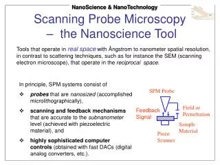
Operation of a Scanning Probe Microscope • Scanning with sub-Angstrom precision • Probe detection (e.g., current, force, position, …) • Electronicsprocessing • Computer control • Image processing • Vibration isolation • Environmental control (e.g., vacuum, atmosphere, fluid; temperature)
Scanning Tunneling Microscope Omicron
Tunneling • One-dimensional tunneling • Density of electronic statesof sample and tip = sample wavefunction = tip wavefunction = workfunction
Forces Typical: Contact vs. non-contact modes ... Forces to atto-newton (10-18 N) range ...
Themes • IMAGING • INTERROGATING • MANIPULATING atoms and nanoscale objects
IMAGING ATOMS AND NANOSCALE OBJECTS
Large-scale Atomic-scale Gold Grating 30 µm 30 µmSTM Graphite 4.2 nm 4.2 nmSTM DiNardo
Semiconductor Surfaces - Si(100) Tilted dimer SymmetricDimer Unreconstructed L) OccupiedR) Unoccupied Hamers, 1986
Temperature-dependent Reconstructions • Low-temperature Si(100)-c(42) vs. (2 1) • Domain boundaries, p(2 2) regions Wolkow, 1992
Homoepitaxial Growth - Si(100) Mo, 1988
Fractional Images • Probing atomic orbitals • Frequency-modulatedAtomic Force Microscopy • Si tip / Si(111)-77 Si atom Giessibl, 2000
Metal Surfaces Wahlström, 1998
0.4 ML Ag/Cu(110) c(102) model a, b) 230230 nm2 c) 5.45.4 nm2 d) 3.83.8 nm2 Sprunger, 1996
Interfaces - Cross-sectional Imaging Ohmori, 1999
Molecular Adsorption - CO/Pt(111) Pederson, 1996
Faulted Layer Orientation Change Interstitial Defect Recovery Line Defect Vacancy Coatings - Colloidal Latex Particles Brennan, 2000
Carbon Nanotubes Odom, 1998
Overlapping Nanotubes Avouris, 1999
Nanotube Shapes and Forces Avouris, 1999
Biological Macromolecules - Collagen Brennan, 2000
Biological Macromolecules - Fibronectin Brennan, 1999
INTERROGATING ATOMS AND NANOSCALE OBJECTS
Visualizing the Tunnel JunctionSTM-TEM Naitoh, 1996
Scanning Ohnishi, 1998
Bias-dependent imaging ~ GaAs(110) • GaAs(110) (cleaved) surface Feenstra, 1987
Spectroscopy ~ on the Nanoscale • Beam techniques average over surface species • SPM techniques measure density of states related to the atom (or molecule) under the tip • electronic spectrum - measure dI/dV [or (dI/dV)/(I/V)] Hamers, 1986
Electronic SpectroscopyAtom by Atom • Reconstructed Si(100)-21 surface • Dimers • Occupied electronic states of dimers (between atoms) • Unoccupied electronic states of dimers (away from atoms) Hamers, 1986
Defects • Atomic-sized defects • Al/Si(111)-√3√3 structure • different electronic states Hamers, 1988
Chemical Reactivity NH3 reacted with the Si(111)-77 surface Wolkow, 1988
Vibrational SpectroscopyMolecule by Molecule Lauhon, 2000
Chemical Reactions Electron-induced dissociation product -pyridine on Cu(100) at 8K Lauhon, 2000
Surface DiffusionChasing Atoms with the Atom Tracker Swartzentruber, 1996
H-enhanced diffusion of Pt atoms an STM movie ... Horch, 1999
Electrostatic Force Microscopy (EFM) • Application • Topography of integrated circuit • Monitoring an active integrated circuit Digital Instruments, www.di.com
Scanning Capacitance Microscopy Nakakura, 1999
Magnetic Force Microscopy (MFM) • Magnetic tip interaction with surface • Application: Disk drive • Morphology • Magnetic structure Digital Instruments, www.di.com
Scanning Chemical Microscopy • Measure chemical interaction between the tip and sample • Functionalize the tip with hydrophobic or hydrophilic species • Scan over surface and measure adhesion force or friction force
Carbon Nanotube Tips- Functionalization - Wong, 1998
Scanning Chemical Microscopy Frisbee, 1994 / Wong, 1998
Adhesion Forces Wong, 1998
Friction Force Microscopy • Macroscopic friction forces • Microscopic friction forces
Polymer Thin Films Polypropylene film (a) AFM + (b) FFM, (c) non-contact AFM Nie, 1999