Download
1 / 44
480 likes | 926 Views
Scanning Probe Microscopy Nanoscience and Nanotechnology. Huixin He Room 234, Olson Hall Phone: 973-353-1254 Email: huixinhe@newark.rutgers.edu. Lecture notes will be found at:. http://andromeda.rutgers.edu/~huixinhe/courses/course.html. Scanning probe microscopy.

E N D
Scanning Probe Microscopy Nanoscience and Nanotechnology Huixin He Room 234, Olson Hall Phone: 973-353-1254 Email: huixinhe@newark.rutgers.edu Lecture notes will be found at: http://andromeda.rutgers.edu/~huixinhe/courses/course.html Scanning probe microscopy
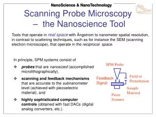
The goal of the course will be to introduce the SPM technique and the frontiers research in nanoscience and technology in ways that a broad range of students can appreciate and use “nanoconcepts” and the SPM technique in their own research. The focus of the course will be on the use of scanning probe microscopy to extend the scope of traditional areas of research to the revolutionary nanoscience research and the state-of-art nanotechnology
The learning goal of this course is the basic operation of atomic force microscope, and operation principle of several basic imaging modes in the family of scanning probe microscopy and their advanced applications.
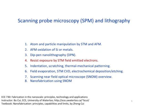
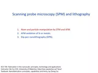
Tentative Syllabus and Topics ( may change slightly as we proceed through the semester) • Overview of scanning probe microscopy, working principles of STM and AFM and some important parts in the instruments. • Hands on experience of atomic force microscope • Toward imaging with the theoretical resolutions. • More working principles for new imaging mode and their applications • In-situ electrochemistry of AFM and STM • Application beyond imaging (1) Nanoelectronics and molecular electronics • Application beyond imaging (2) Nanofabrication • Application beyond imaging (3) Single molecular force spectroscopy • Application beyond imaging (4) Nanomechanics/chemical and biochemical detection.
Textbooks • There is no prescribed textbook for the course. Some reference books and materials are listed below, but more will be provided before each lecture. • “Scanning Probe Microscopy and Spectroscopy, theory, techniques and applications” Dawn Bonnell 2001 • “Scanning Probe Microscopy and Spectroscopy, Methods and applications” Roland Wiesendanger 1994 • “Atomic Force Microscopy for Biologists” V. J. Morris 1999 • “Intermolecular Surface Forces", J. Israelachvili, Academic Press, 1991 • “Micro/Nanotribology and its applications” Bharat Bhushan 1997. • “Electrochemical nanotechnology” W.J. Lorenz and W. Plieth 1998
Nanoscience and Nanotechnology • How big is “ Nano” ? give some examples which are naturally on • the range of nano? • Could you give some examples how nanoscience and • nanotechnology impact our social and economic life? • Both positive and negative. • What is the excellent tool for the research of nanoscience?
Scanning Probe Microscopy Family: AFM, STM, FFM, EFM, MFM etc.
A blind man is reading! ( without light, but touching) Brain braille braille braille braille braille braille braille braille braille braille Scanning Probe Microscopy How does it work? Compared to other microscopy, this is the only technique could let you “see”
A brief history of SPM: • Scanning Tunneling Microscope (STM) • • Developed in 1981 by Binning, Rohrer, Gerber, and Weibel • at IBM in Zurich, Switzerland. • Gerd Binnig and Heinrich Rohrer have been awarded the • Nobel Prize in Physics 1986 • Atomic Force Microscope (AFM) • • Developed in 1986 by Binning, Quate, and Gerber as a collaboration • between IBM and Stanford University.
SPM family • Scanning Tunneling Microscopy (STM) • • Atomic Force Microscopy (AFM) (Scanning Force Microscopy (SFM) • There are 3 primary modes of AFM: • •Contact Mode AFM • •Non-contact Mode AFM • •TappingMode™ AFM • Lateral Force Microscopy (LFM) • Force Modulation Microscopy • Magnetic Force Microscopy (MFM) • Electric Force Microscopy (EFM) • Surface Potential Microscopy • Phase Imaging • Force Volume
Conitnue… • Electrochemical STM & AFM (ECM) • Scanning Capacitance Microscopy (SCM) • Conductive AFM ( TUNA) • Peakforce imaging • ******************** • Scanning Thermal Microscopy (SThM) • Near-field Scanning Optical Microscopy (NSOM or SNOM) • Photon Scanning Tunneling Microscopy (PSTM) • Ballistic Electron Emission Microscopy (BEEM)
In-situ Electrochemistry Au (111) surface Cu UPD on Au ( 111) surface, In situ electrochemical STM
Nanofabrication Au nanodots array The Logo of Peking University indented on an Au-Pd film with a modification force of 20 nN
To Probe the electronic behavior of single molecules —Molecular Electronics SPM tip (sensitive current measurement)
Molecular Sensors —Single Molecular Recognition SPM tip Attractive force Ligand Receptor Sensitive force measurement
Major components of AFM • AFM tip/cantilever assembly • Force detection system • Electronic Feedback system • Scanner ( precise position control system) • Vibration damping system
AFM tip, the sharpness determined the resolution of imaging Materials: Si or Si3N4 Hard, wear resistant, suit for microfabrication
Carbon Nanotube sharpened Tip Carbon Nanotube Tips: High-Resolution Probes for Imaging Biological Systems Charles M. Lieber JACS, 1998, 120, 603
x1 x2 Force Detection system Hook’ law: F= - kx k: Spring constant of the cantilever Materials, and dimension of the cantilever k increases with lever thickness, decreases with lever length
Photodetector: photodiode, turns light into Electrical signal Mechanically amplification Meyuer, H andAmer, N. M. (1988) “ Novel approach to atomic Force microscopy” Appl. Phys. Lett. 53, 1045-1047 Amplification is determined by the size of the cantilever; The shorter, the larger the angular displacement of the laser beam In theory: 4x10 -4 Å In practice: random thermal excitation of the cantilever
Piezoelectric Scanners (Scanning Mechanism ) Piezoelectric effect: piezoelectric crystals The electrical polarization produces is proportional to the stress and the direction. The polarization changes if the stress changes from compression to tension Reverse piezoelectric effect Materials: lead zirconate titanates ( Pb(Ti, Zr)O3) PZT type )
Linear relationship between L and V Senstivity hysteresis
Vibration isolation— Crucial to obtaining high resolution image SPM by nature is sensitive to very small displacement of The sample or tip. Building vibration, speaking voice, walking… Temperature
Atomic Force Microscopy Force mapping
Very rough surface Tip crashed or sample destroyed Smarter imaging ---Need a Feedback system
Youtube: AFM Principle - How AFM Works AFM_animation_Vo02.wmv