Download
1 / 37
380 likes | 515 Views
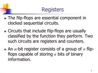
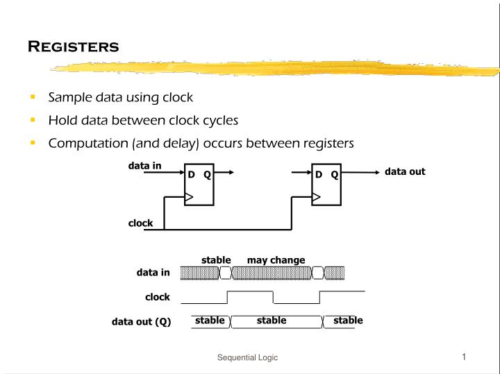
D. D. Q. Q. Registers. Sample data using clock Hold data between clock cycles Computation (and delay) occurs between registers. data in. data out. clock. stable. may change. data in. clock. stable. stable. stable. data out (Q). D. D. Q. Q. T su. T h. input. clock.

E N D
D D Q Q Registers • Sample data using clock • Hold data between clock cycles • Computation (and delay) occurs between registers data in data out clock stable may change data in clock stable stable stable data out (Q) Sequential Logic
D D Q Q Tsu Th input clock Timing Methodologies (cont’d) • Definition of terms • setup time: minimum time before the clocking event by which the input must be stable (Tsu) • hold time: minimum time after the clocking event until which the input must remain stable (Th) data clock there is a timing "window" around the clocking event during which the input must remain stable and unchanged in order to be recognized stable changing data clock Sequential Logic
Tsu2ns Th1ns D Tsu2ns Th1ns CLK Tw 7ns Q Tplh[2,4]ns Tphl[1,3]ns Typical timing specifications • Positive edge-triggered D flip-flop • setup and hold times • minimum clock width • propagation delays (low to high, high to low, max and typical) all measurements are made from the clocking event that is, the rising edge of the clock Sequential Logic
System Clock Frequency • Register transfer must fit into one clock cycle • reg tpd + C.L. tpd + reg tsu < Tclk • Use maximum delays • Find the “critical path” • Longest register-register delay Sequential Logic
Short Paths • Can a path have too little delay? • Yes: Hold time can be violated • Unless tpd > th • Use min delay (contamination delay) • Fortunately, most registers have hold time = 0 • But there can still be a problem! Clock skew… Sequential Logic
Clock Skew • Cannot make clock arrive at registers at the same time • If skew > 0: • tpd > th + tskew • Clock skew can cause system failure • Can you fix this after you’ve fabbed the chip? Sequential Logic
Clock Skew • Cannot make clock arrive at registers at the same time • If skew > 0: • tpd > th + tskew • Clock skew can cause system failure • Can you fix this after you’ve fabbed the chip? Sequential Logic
Clock Skew • If skew < 0: • tclk > reg tpd + CL tpd + reg tSU + |tskew| • Can you fix this after fab? Sequential Logic
Clock Skew • If skew < 0: • tclk > reg tpd + CL tpd + reg tSU + |tskew| • Can you fix this after fab? Sequential Logic
Clock Skew • Correct behavior assumes that all storage elements sample at exactly the same time • Not possible in real systems: • clock driven from some central location • different wire delay to different points in the circuit • Problems arise if skew is of the same order as FF contamination delay • Gets worse as systems get faster (wires don't improve as fast) • 1) distribute clock signals against the data flow • 2) wire carrying the clock between two communicating components should be as short as possible • 3) try to make all wires from the clock generator be the same length => clock tree Sequential Logic
Nasty Example • What can go wrong? • How can you fix it? Sequential Logic
Other Types of Latches and Flip-Flops • D-FF is ubiquitous • simplest design technique, minimizes number of wires preferred in PLDs and FPGAs good choice for data storage register edge-triggered has most straightforward timing constraints • Historically J-K FF was popular versatile building block, often requires less total logic two inputs require more wiring and logic can always be implemented using D-FF • Level-sensitive latches in special circumstances popular in VLSI because they can be made very small (4 T) fundamental building block of all other flip-flop types two latches make a D-FF • Preset and clear inputs are highly desirable • System reset Sequential Logic
D Q D Q Comparison of latches and flip-flops D CLK Qedge Qlatch CLK positiveedge-triggeredflip-flop CLK transparent, flow-through(level-sensitive)latch behavior is the same unless input changes while the clock is high Sequential Logic
What About External Inputs? • Internal signals are OK • Can only change when clock changes • External signals can change at any time • Asynchronous inputs • Truly asynchronous • Produced by a different clock • This means register may sample a signal that is changing • Violates setup/hold time • What happens? Sequential Logic
Sampling external inputs Sequential Logic
Synchronization failure • Occurs when FF input changes close to clock edge • the FF may enter a metastable state – neither a logic 0 nor 1 – • it may stay in this state an indefinite amount of time • this is not likely in practice but has some probability logic 1 logic 0 logic 0 logic 1 oscilloscope traces demonstrating synchronizer failure and eventual decay to steady state small, but non-zero probability that the FF output will get stuck in an in-between state Sequential Logic
Calculating probability of failure • For a single synchronizer Mean-Time Between Failure (MTBF) = exp ( tr / ) / ( T0 fc fa )where a failure occurs if metastability persists beyond time tr • tr is the resolution time - extra time in clock period for settling • Tclk - (tpd + TCL + tsetup) • fc is the frequency of the FF clock • fa is the number of asynchronous input changes per second applied to the FF • T0 and are constaints that depend on the FF's electrical characteristics (e.g., gain or steepness of curve) • example values are T0 = 1ms and = 30ps (sensitive to temperature, voltage, cosmic rays, etc.). • Must add probabilities from all synchronizers in system 1/MTBFsystem = 1/MTBFsynch Sequential Logic
Xilinx Measurements Sequential Logic
Xilinx Measurements Sequential Logic
What does this circuit do? • What’s wrong with this? Sequential Logic
What does this circuit do? • How much better is this? • Can you do better? Sequential Logic
Guarding against synchronization failure • Give the register time to decide • Probability of failure cannot be reduced to 0, but it can be reduced • Slow down the system clock? • Use very fast technology for synchronizer -> quicker decision? • Cascade two synchronizers? Q asynchronous input synchronized input D Q D Clk Sequential Logic
Stretching the Resolution Time • Also slows the sample rate and transfer rate Sequential Logic
Sampling Rate • How fast does your sample clock need to be? Sequential Logic
Sampling Rate • How fast does your sample clock need to be? • f(clkB) > f(clkA) • f(clkB) > 2 f(data) (Nyquist) Sequential Logic
Sampling Rate • What if sample clock can’t go faster? • If input clock is not available, no solution(?) • If input clock is available (e.g. video codec) Sequential Logic
Increasing sample rate • The problem is the relative sample rate • Slow down the input clock! Sequential Logic
Another Problem with Asynchronous inputs • What goes wrong here? (Hint: it’s not a metastability thing) • What is the fix? Sequential Logic
More Asynchronous inputs • What is the problem? • What is the fix? Sequential Logic
Important Rule! • Exactly one register makes the synchronizing decision Sequential Logic
More Asynchronous inputs • Can we input asynchronous data values with several bits? Sequential Logic
More Asynchronous inputs • How can we input asynchronous data values with several bits? Sequential Logic
What Went Wrong? • Each bit has a different delay • Wire lengths differ • Gate thresholds differ • Driver speeds are different • Register delays are different • Rise vs. Fall times • Clock skews to register bits • Bottom line – “data skew” is inevitable • aka Bus Skew • Longer wires => More skew • What is the solution?? Sequential Logic
Sending Multiple Data Bits • Must send a “clock” with the data • Waits until data is stable • De-skewing delay • f(clkB) > 2 f(clkA) Sequential Logic
Sending Multiple Data Bits • Balancing path delays . . . • What’s wrong with this solution? • What’s the right way to do it? Sequential Logic
Sending Multiple Data Bits • The right way to do it . . . Sequential Logic
Sending Multiple Data Bits • Slightly different alternative . . . Sequential Logic