Download

1 / 17
190 likes | 365 Views
Registers. Overview. Parallel Load Register Shift Registers Serial Load Serial Addition Shift Register with Parallel Load Bidirectional Shift Register VHDL representation of Shift Register. Registers and Counters.

E N D
Overview • Parallel Load Register • Shift Registers • Serial Load • Serial Addition • Shift Register with Parallel Load • Bidirectional Shift Register • VHDL representation of Shift Register Chapter 5-i: Registers (5.1-5.3, 5.7)
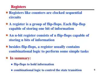
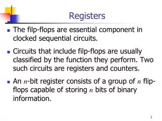
Registers and Counters • A n-bit register is a set of n flip-flops that is capable of storing n bits of binary information. • With added combinational gates, the register can perform data-processing tasks. • A counter is a register that goes through a predetermined sequence of states upon the application of clock pulses. Chapter 5-i: Registers (5.1-5.3, 5.7)
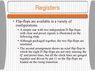
Registers • Example (next slide) generic 4-bit register. • The common Clock input triggers all flip-flops on the rising edge of each pulse, and the binary data available at the four D inputs are transferred into the 4-bit register. Chapter 5-i: Registers (5.1-5.3, 5.7)
Registers with parallel load • Next page shows a 4-bit register with a control input Load that is directed through gates into the D inputs of the flip-flops. • When Load is 1, the data on the four inputs is transferred into the register with the next positive transition of a clock pulse. • When Load is 0, the data inputs are blocked, and the D inputs of the flip-flops are connected to their outputs. Chapter 5-i: Registers (5.1-5.3, 5.7)
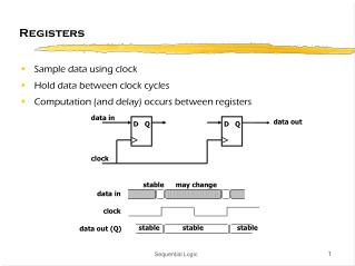
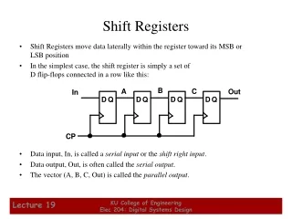
Shift registers • A register capable of shifting its stored bits laterally in one or both directions is called a shift register. • The logical configuration of a shift register consists of a chain of flip-flops in cascade, with the output of one flip-flop connected to the input of the next FF. Chapter 5-i: Registers (5.1-5.3, 5.7)
Shift Register Chapter 5-i: Registers (5.1-5.3, 5.7)
Shift registers (cont.) • The next figure shows how the serial transfer of information from register A to register B can be done. One clock cycle per bit of data is required. Chapter 5-i: Registers (5.1-5.3, 5.7)
Serial data transfer Chapter 5-i: Registers (5.1-5.3, 5.7)
Serial addition using shift registers • The two binary numbers to be added serially are stored in two shift registers. • Bits are added one pair at a time through a single full-adder circuit. • The carry out of the full adder is transferred into a D flip-flop. The output of the carry FF is then used as the carry input for the next pair of bits. • The sum bit on the S output of the full adder is transferred into the result register A. Chapter 5-i: Registers (5.1-5.3, 5.7)
Serial vs. parallel addition • The parallel adder is a combinational circuit, whereas the serial adder is a sequential circuit. • The parallel adder has n full adders for n-bit operands, whereas the serial adder requires only one full adder. • The serial circuit takes n clock cycles to complete an addition. • In summary, the parallel adder in space is n times larger than the serial adder, but it is n times faster. • The serial adder, although it is n times slower, is n times smaller in space. Chapter 5-i: Registers (5.1-5.3, 5.7)
Shift register with parallel load Chapter 5-i: Registers (5.1-5.3, 5.7)
Shift register with parallel load Chapter 5-i: Registers (5.1-5.3, 5.7)
Bidirectional shift register Chapter 5-i: Registers (5.1-5.3, 5.7)
Bidirectional Shift Register Chapter 5-i: Registers (5.1-5.3, 5.7)