Registers
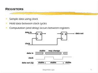
Registers. Flip-flops are available in a variety of configurations. A simple one with two independent D flip-flops with clear and preset signals is illustrated on the following slide. Although packaged together, the two flip-flops are unrelated.

Registers
E N D
Presentation Transcript
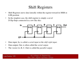
Registers • Flip-flops are available in a variety of configurations. • A simple one with two independent D flip-flops with clear and preset signals is illustrated on the following slide. • Although packaged together, the two flip-flops are unrelated. • The second arrangement shows an octal flip-flop in which the eight D flip-flops are not only missing the Q’ and preset lines, but all the clock lines are ganged together and driven by pin 11 so the flip-flops are loaded on the rising transition.
Registers • All eight clear signals are also ganged, so when pin 1 goes to 0, all the flip-flops are forced to their 0 state. • While one reason, for ganging the clock and clear lines is to save pins, the chip in this case is used in a different way from eight unrelated flip-flops. It is used as a single 8-bit register. • We can also use two such chips as a 16-bit register by tying their respective pins 1 and 11 together.
Memory Organization • To build large memories a different organization is required, one in which individual words can be addressed. • One such organization that meets this criterion is shown on the next slide. • This example shows a memory with four 3-bit words. Each operation reads or writes a full 3-bit word. The organization requires fewer pins then an octal flip-flop and extends easily to large memories. • The memory has eight input lines and three output lines.
Memory Organization • We could have designed a circuit in which the three OR lines were just fed into the the three output lines, but in practice the same lines are used for both input and output. • What is needed is an electronic switch that can make or break a connection in a few nanoseconds. Such a switch is called a noninverting buffer. It has a data in, data out, and a control line. When control is high, the buffer acts like a wire. When control is low, the buffer acts like an open circuit.
Memory Organization • An inverting buffer acts like a normal buffer when control is high, and disconnects the output from the circuit when control is low. • Both kinds of buffers are tri-state devices, because they can output 0, 1, or none of the above. • Buffers also amplify signals so they can drive many output simultaneously. • They are sometimes used in circuits for this reason, even when their switching properties are not needed.
Memory Chips • The memory shown previously easily extends to larger sizes. • For example, to extend to 4 words of 8 bits each we add five more columns of four flip-flops each, as well as five more input and output lines. To extend to eight words of three bits each, we add four more rows of three flip-flops each and one more address line. • For maximum efficiency, the number of words in memory should be a power of 2, but the size of words can be anything.
Memory Chips • For any given memory size, there are various ways of organizing the chip. • A 4-Mbit chip could be organized as 512K words of 8 bits each or 4096K words of 1 bit each. • Aside - on some pins a high voltage causes an action to happen while on others a low voltage causes the action. Thus, we will say that a signal is asserted or negated to avoid this issue. A signal S is asserted high, but S’ is asserted low.
Memory Chips • Since a computer will generally have multiple memory chips, a signal is needed to select the chip that is currently needed. The CS’ (Chip Select) signal is provided for this purpose. • We also a need a signal to distinguish reads from writes - the WE’ (Write Enable) signal. • The OE’ (Output Enable) signal is asserted to drive the output signals. When it is not asserted, the chip output is disconnected.
Memory Chips • An alternative addressing scheme is used in the second chip organization of the previous slide. • To address the chip, first a row is selected by putting its 11-bit number on the address pins. Then the RAS’ (Row Address Strobe) is asserted. • Then a column number is put on the address pins and CAS’ (Column Address Strobe) is asserted. A single bit is read or written. • This reduces the number of pins required, but we need to clock cycles to address memory.
RAMs and ROMs • The memories we have seen can be both read and written. Such memories are called RAMs (Random Access Memories). • RAMs come in two varieties, static and dynamic. • Static RAMs (SRAMs) are constructed using circuits similar to the D flip-flop. They retain memory as long as power is on, are fast, and are often used to implement level 2 cache memory.
RAMs and ROMs • Dynamic RAMs (DRAMs) do not use flip-flops. A DRAM is an array of cells, each cell contains one transistor and one capacitor. The capacitors can be charged or discharged, allowing data to be stored. • Since the electric charge tends to leak away, every bit in a DRAM must be refreshed every few milliseconds. DRAMs have a high capacity, thus they are almost always used for main memory. On the other hand, they are slow.
RAMs and ROMs • An FPM (Fast Page Mode) DRAM is organized as a matrix of bits and requires a row and then a column address to be presented. • FPM DRAM is gradually being replaced by EDO (Extended Data Output) DRAM, which allows a second memory reference to begin before the previous memory reference completes. • Both FPM and EDO chips are asynchronous (the address and data lines are not driven by a single clock).
RAMs and ROMs • SDRAM (Synchronous DRAM) is a hybrid of static and dynamic RAM and is driven by a single synchronous clock. It is often used in large caches. • ROMs (Read-Only Memories) have their data inserted during manufacture . The only way to replace the program in a ROM is to replace the chip. • The PROM (Programmable ROM) can be programmed (once) in the field by selectively blowing fuses.
RAMs and ROMs • The EPROM (Erasable PROM) can be field-erased as well by exposing the EPROM to a strong ultraviolet light for 15 minutes. • The EEPROM can be erased by applying pulses to it rather than UV light. It can also be programmed in place (an EPROM requires a special programming device). EEPROMs are slow compared to DRAMs and SRAMs. • Flash memory is block erasable and rewritable. They are often used in digital cameras, but they wear out after about 10,000 erasures.
CPU Chips • All modern CPUs are contained on a single chip. • Each CPU chip has a set of pins, through which all communications with the outside world occur. • The pins on a CPU chip can be divided into three types: • address • data • control
CPU Chips • These pins are connected to similar pins on the memory and I/O chips via a collection of parallel wires called a bus. • To fetch an instruction from memory, the CPU: • puts the memory address of the instruction on its address pins • asserts one or more control lines to inform the memory that it wants to read a word • waits for a signal from the memory that it has put the data on the CPU’s data pins • accepts the word and carries out the instruction
CPU Chips • Two of the key parameters that determine the performance of a CPU are the number of address pins and the number of data pins. • A chip with m address pins can address up to 2m memory locations. • A chip with n data pins can read or write an n-bit word in a single operation. • A CPU with 8 data pins will take four operations to read a 32-bit word, whereas one with 32 data pins takes just one operation. More pins implies more expensive, however.