Download
1 / 26
270 likes | 815 Views
Discover the essentials of registers in digital systems design, their functions, types, and implementation models. Learn about register storage, transfer operations, design strategies, and more in this comprehensive guide.

E N D
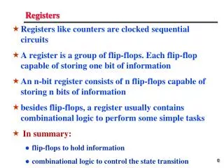
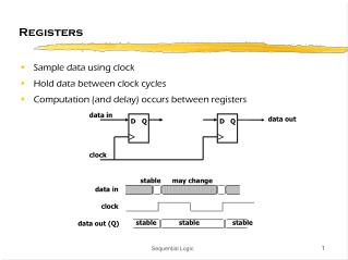
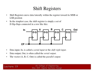
Registers • Register – a collection of binary storage elements • In theory, a register is sequential logic which can be defined by a state table • More often think of a register as storing a vector of binary values • Frequently used to perform simple data storage and data movement and processing operations KU College of Engineering Elec 204: Digital Systems Design
A1 Y1 In1 Q D C A0 Y0 In0 Q D CP C Current Next State Output State A1(t+ 1 ) A0(t+ 1 ) (=A1 A0) For I1 I0 = A1 A0 00 01 10 11 Y1 Y0 0 0 00 01 10 11 0 0 0 1 00 01 10 11 0 1 1 0 00 01 10 11 1 0 1 1 00 01 10 11 1 1 Example: 2-bit Register • How many states are there? • How many input combinations?Output combinations • What is the output function? • What is the next state function? • Moore or Mealy? • What are the the quantities above for an n-bit register? KU College of Engineering Elec 204: Digital Systems Design
Register Design Models • Due to the large numbers of states and input combinations as n becomes large, the state diagram/state table model is not feasible! • What are methods we can use to design registers? • Add predefined combinational circuits to registers • Example: To count up, connect the register flip-flops to an incrementer • Design individual cells using the state diagram/state table model and combine them into a register • A 1-bit cell has just two states • Output is usually the state variable KU College of Engineering Elec 204: Digital Systems Design
Register Storage • Expectations: • A register can store information for multiple clock cycles • To “store” or “load” information should be controlled by a signal • Reality: • A D flip-flop register loads information on every clock cycle • Realizing expectations: • Use a signal to block the clock to the register, • Use a signal to control feedback of the output of the register back to its inputs, or • Use other SR or JK flip-flops which for (0,0) applied store their state • Load is a frequent name for the signal that controls register storage and loading • Load = 1: Load the values on the data inputs • Load = 0: Store the values in the register KU College of Engineering Elec 204: Digital Systems Design
Gated Clock = Clock + Load Registers with Clock Gating • Load signal is used to enable the clock signal to pass through if 1 and prevent the clock signal from passing through if 0. • Example: For Positive Edge-Triggered or Negative Pulse Master-Slave Flip-flop: • What logic is needed for gating? • What is the problem? Clock Load Gated Clock to FF Clock Skew of gated clocks with respect to clock or each other KU College of Engineering Elec 204: Digital Systems Design
Registers with Load-Controlled Feedback • A more reliable way to selectively load a register: • Run the clock continuously, and • Selectively use a load control to change the register contents. • Example: 2-bit registerwith Load Control: • For Load = 0,loads register contents(hold current values) • For Load = 1,loads input values(load new values) • Hardware more complexthan clock gating, butfree of timing problems 2-to-1 Multiplexers A1 Y1 Q D Load In1 C A0 Y0 Q D C In0 Clock KU College of Engineering Elec 204: Digital Systems Design
Register Transfer Operations • Register Transfer Operations – The movement and processing of data stored in registers • Three basic components: • set of registers • operations • control of operations • Elementary Operations -- load, count, shift, add, bitwise "OR", etc. • Elementary operations called microoperations KU College of Engineering Elec 204: Digital Systems Design
R 7 6 5 4 3 2 1 0 15 8 7 0 15 0 PC(H) PC(L) R2 Register Notation • Letters and numbers – denotes a register (ex. R2, PC, IR) • Parentheses ( ) – denotes a range of register bits (ex. R1(1), PC(7:0), AR(L)) • Arrow () – denotes data transfer (ex. R1 R2, PC(L) R0) • Comma – separates parallel operations • Brackets [ ] – Specifies a memory address (ex. R0 M[AR], R3 M[PC] ) KU College of Engineering Elec 204: Digital Systems Design
K 1 Load n R1 R2 Clock Clock K1 Transfer Occurs Here No Transfers Occur Here Conditional Transfer • If (K1 =1) then (R2 R1) is shortened to K1: (R2 R1) where K1 is a control variable specifying a conditional executionof the microoperation. KU College of Engineering Elec 204: Digital Systems Design
Microoperations • Logical Groupings: • Transfer - move data from one set of registers to another • Arithmetic - perform arithmetic on data in registers • Logic - manipulate data or use bitwise logical operations • Shift - shift data in registers Arithmetic operations+ Addition– Subtraction* Multiplication/ Division Logical operations Logical OR Logical AND Logical Exclusive OR Not KU College of Engineering Elec 204: Digital Systems Design
Example Microoperations • Add the content of R1 to the content of R2 and place the result in R1. R1 R1 + R2 • Multiply the content of R1 by the content of R6 and place the result in PC. PC R1 * R6 • Exclusive OR the content of R1 with the content of R2 and place the result in R1. R1 R1 R2 KU College of Engineering Elec 204: Digital Systems Design
Example Microoperations (Continued) • Take the 1's Complement of the contents of R2 and place it in the PC. • PC R2 • On condition K1 OR K2, the content of R1 is Logic bitwise Ored with the content of R3 and the result placed in R1. • (K1 + K2): R1 R1 R3 • NOTE: "+" (as in K1 + K2) and means “OR.” In R1 R1 + R3, + means “plus.” KU College of Engineering Elec 204: Digital Systems Design
Control Expressions • Example:X K1 : R1 R1 + R2X K1 : R1 R1 + R2 + 1 • Variable K1 enables the add or subtract operation. • If X =0, then X =1 so X K1 = 1, activating the addition of R1 and R2. • If X = 1, then X K1 = 1, activating the addition of R1 and the two's complement of R2 (subtract). • The control expression for an operation appears to the left of the operation and is separated from it by a colon • Control expressions specify the logical condition for the operation to occur • Control expression values of: • Logic "1" -- the operation occurs. • Logic "0" -- the operation does not occur. KU College of Engineering Elec 204: Digital Systems Design
Arithmetic Microoperations Symbolic Designation Description ¬ Addition R0 R1 + R2 • FromTable7-3: • Note that any register may be specified for source 1, source 2, or destination. • These simple microoperations operate on the whole word ¬ R1 Ones Complement R0 ¬ Two's Complement R0 R1 + 1 ¬ R2 minus R1 (2's Comp) R0 R2 + R1 + 1 ¬ Increment (count up) R1 R1 + 1 ¬ Decrement (count down) R1 R1 – 1 KU College of Engineering Elec 204: Digital Systems Design
Ex: • X’K1: R1 R1 + R2 • X K1: R1 R1 + R2’ + 1 • K1: activates operation • X : picks add or subtr KU College of Engineering Elec 204: Digital Systems Design
Logical Microoperations • From Table 7-4: Symbolic Description Designation ¬ Bitwise NOT R0 R1 ¬ Ú Bitwise OR (sets bits) R0 R1 R2 ¬ Bitwise AND (clears bits) R0 R1 R2 Ù ¬ Å Bitwise EXOR (complements bits) R0 R1 R2 KU College of Engineering Elec 204: Digital Systems Design
Logical Microoperations (continued) • Let R1 = 10101010, and R2 = 11110000 • Then after the operation, R0 becomes: KU College of Engineering Elec 204: Digital Systems Design
Symbolic Description Designation ¬ Shift Left R1 sl R2 ¬ Shift Right R1 sr R2 R1 Operation ¬ 10010010 R1 sl R2 ¬ 01100100 R1 sr R2 Shift Microoperations • From Table 7-5: • Let R2 = 11001001 • Then after the operation, R1 becomes: • Note: These shifts "zero fill". Sometimes a separate flip-flop is used to provide the data shifted in, or to “catch” the data shifted out. • Other shifts are possible (rotates, arithmetic). KU College of Engineering Elec 204: Digital Systems Design
Register Transfer Structures • Multiplexer-Based Transfers - Multiple inputs are selected by a multiplexer dedicated to the register • Bus-Based Transfers - Multiple inputs are selected by a shared multiplexer driving a bus that feeds inputs to multiple registers • Three-State Bus - Multiple inputs are selected by3-state drivers with outputs connected to a bus that feeds multiple registers • Other Transfer Structures - Use multiple multiplexers, multiple buses, and combinations of all the above KU College of Engineering Elec 204: Digital Systems Design
Load K 2 R2 K 1 Load S n 0 n R0 MUX n Load 1 R1 Multiplexer-Based Transfers • Multiplexers connected to register inputs produce flexible transfer structures (Note: Clocks are omitted for clarity) • The transfers are: K1: R0 R1 K2 K1: R0 R2 KU College of Engineering Elec 204: Digital Systems Design
Multiplexer and Bus-Based Transfers for Multiple Registers • Multiplexer dedicated to each register • Shared transfer paths for registers • A shared transfer object is a called a bus (Plural: buses) • Bus implementation using: • multiplexers • three-state nodes and drivers • In most cases, the number of bits is the length of the receiving register KU College of Engineering Elec 204: Digital Systems Design
Multiplexer Approach • Uses an n-input multiplexer with a variety of transfer sources and functions KU College of Engineering Elec 204: Digital Systems Design
Multiplexer Approach • Load enable by OR of control signals K0, K1, … Kn-1- assumes no load for 00…0 • Use: • Encoder + Multiplexer (shown) or • n x 2 AND-OR to select sources and/ortransfer functions KU College of Engineering Elec 204: Digital Systems Design
L0 S0 Load S n n 0 MUX n R0 1 L1 S1 Load S n n 0 MUX n R1 1 L2 S2 Load S n n 0 MUX n R2 1 Dedicated MUX-Based Transfers • Multiplexer connected to each register input produces a very flexible transfer structure => • Characterize the simultaneous transfers possible with this structure. KU College of Engineering Elec 204: Digital Systems Design
Load n R0 S1 S0 L1 S1 S0 n 0 Load n n n 1 MUX n R1 2 L2 Load n R2 Multiplexer Bus L0 • A single bus driven by a multiplexer lowers cost, but limits the available transfers => • Characterize the simultaneous transfers possible with this structure. • Characterize the cost savings compared to dedicated multiplexers KU College of Engineering Elec 204: Digital Systems Design
L0 Load n R0 n E0 L1 Load n R1 n E1 L2 Load n R2 n E2 Three-State Bus • The 3-input MUX can be replaced by a 3-state node (bus) and 3-state buffers. • Cost is further reduced, but transfers are limited • Characterize the simultaneous transfers possible with this structure. • Characterize the cost savings and compare • Other advantages? KU College of Engineering Elec 204: Digital Systems Design