Download
1 / 43
430 likes | 535 Views
Explore the history, hardware, and software evolution of Sun Microsystems, focusing on the UltraSPARC-III Processor's architecture and design goals, performance, and scalability. Learn about the company's strategic shifts and current focus.

E N D
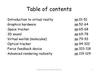
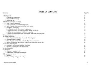
Table of Contents 1 Introduction to Sun Microsystems: Brief history Hardware Software Present Focus 2 Ultra SPARC-III Processor: Introduction Architecture design goals Compatibility Performance Scalability Reliability Major architectural units Instruction Pipeline (Instruction Issue Unit-Integer Execute Unit) On Chip Memory System (Data Cache Unit) Floating Point Unit External Memory Unit-System Interface Unit Instruction Pipeline Physical Design Conclusion
Brief history • Sun's products include servers and workstations based on Sun’s own SPARC , the Solarisoperating system, the NFS, and the Java platform • The initial design for Sun's UNIX workstation was conceived when the founders were graduate students at Stanford University, California. • SUN stands for Stanford University Network. The company was incorporated in 1982 and went public in 1986.
Hardware • Sun originally used the Motorola 68000 family then starting with the SPARCstation 1, the company used its processor family, SPARC. • SPARC (Scalable Processor ARChitecture) is a RISC architecture designed in 1985. • Sun has implemented multiple high-end generations of the Sparc architecture, including Sparc-1, SuperSparc, UltraSparc-I, UltraSparc-II, UltraSparc-III, and currently UltraSparc IV.
Hardware continued • The SPARC processor contains 128 general purpose registers divided into 32-register groups. • A 32-register group is divided into 8 global registers and 24 stack of registers. These 24 registers form a register window. Each window has 8 local registers and shares 8 registers with adjacent windows. The shared registers are used for passing function parameters and returning values, and the local registers are used for keeping values across function calls. • The “Scalable” in SPARC comes from the fact that the SPARC specification allows up to 32 register windows. So, we can choose to implement all the 32 to provide maximum call stack efficiency, or to implement minimum to reduce the context switching time. • In version 8, the floating-point register file has 16 double precision registers. Each of them can be used as two single precision registers to provide a total of 32 single precision registers. An odd-even number pair of double precision registers can be used as a quad precision register, thus allowing 8 quad precision registers. Version 9 added 16 more double precision registers, but these additional double precision registers can not be used as single precision registers.
Software • After several years of difficult competition and loss of server market share to Linux-based systems, Sun has offered Linux-based desktop software called Java Desktop System for use both on x86hardware and on Sun's SunRay systems. • Sun has also announced plans to supply its Java Enterprise System on Linux, and to release its newest OS, Solaris 10, under the open-sourceCommon Development and Distribution License.
Present Focus • In 2004, Sun cancelled two major processor projects which were emphasizing high instruction level parallelism and high operating frequency. Instead, the company chose to concentrate on processor projects emphasizing multi-threading and multiprocessing. The company also announced a collaboration with Fujitsu to use it’s processor chips. Finally, it has a strategic alliance with AMD to produce market-leading x86/x64 servers based on AMD's Opteron processor. • In February 2005, Sun announced the Sun Grid , a grid computing deployment on which it offers utility computing services priced at $1 per CPU/hour for processing and per GB/month for storage. This offering builds upon an existing 3,000-CPU supercomputer used for internal R&D for over 10 years. • Sun reported a profit in the recent quarter, the first in the last three years. Sun chooses not to carry most forms of insurance (such as earthquake insurance). • Sun has a growing team of over 1400 design engineer.
Introduction • The UltraSPARC-III is the third generation of Sun. • This design is the heart of systems, ranging from desktop workstations to large servers. • The design permits the scalability to build systems consisting of 1000+ Ultra-SPARC processors. • The design ensures compatibility with all existing SPARC applications and the Solaris OS. • This design is a 64-bit Sun’s SPARC Version 9 architecture. • The UltraSPARC-III design built in CMOS with 7 metal layers for signals, clocks, and power.
Architecture Design Goals • Compatibility (with both the applications and OS’s). • Performance (pushing up the clock rate while scaling down the execution latencies). - As the clock rate scales, the bandwidth (operations/unit time) and latencies (time/operation) are scaled proportionally. - As the load latency increases, the amount of ILP decreases.
Architecture Design Goals continued • Scalability - Eliminating long wires in the design as process geometries decreases. - designing the on-chip memory system and the bus interface to handle multiprocessor systems to be built with from 2 to 1000 UltraSPARC-III processors. • Reliability (high levels of reliability, availability and serviceability RAS to maximize system up time and minimize the time to repair)
Instruction Issue Unit • Feeds the execution pipelines with instructions. • It predicts the control flow through a program and fetches the predicted path from the memory system. • Fetched instructions are staged in a queue before forwarding to the two execution units. • The IIU includes a 32-Kbyte, four-way associative instruction cache, the instruction address translation buffer, and a 16 K-entry branch predictor.
Integer Execute Unit • Executes all integer data type instructions: loads, stores, arithmetics, logicals, shifts, and branches. • Four independent data paths enable up to four integer instructions to be executed per cycle: • 2 from (arithmetic, logical, shift), A0/A1 pipelines • 1 from (load, store), MS pipeline • 1 from (branch), BR pipeline
On-chip memory system (Data Cache Unit ) • It comprises the level-one (L1) on chip cache and the data address translation buffer. • There are three first level, on-chip data caches: Data 64-Kbyte, four-way associative, 32-byte line. Prefetch 2-Kbyte, four-way associative, 64-byte line. Write2-Kbyte, four-way associative, 64- byte line.
Floating Point Unit • Execute all floating-point and graphic data type instructions. • Three data paths concurrently execute floating- point or graphic instructions: · Divide/Multiply. · Add/Subtract/Compare. · An independent division data path, which lets a non pipelined divide proceed concurrently with the fully pipelined multiply and add data paths.
External Memory Unit • This unit controls the two off-chip memory structures: - The level-two (L2) data cache built with off-chip synchronous RAMs (SRAMs). - The main memory system built with off-chip synchronous DRAMs (SDRAMs). • The L2 cache controller includes a 90-Kbyte on-chip tag RAM to support L2 cache sizes up to 8 Mbytes. • The main memory controller can support up to four banks of SDRAM memory totaling 4Gbytes of storage.
System Interface Unit • This unit handles external communication to other processors, memory systems, and I/O devices. • The unit can handle up to 15 transactions to external devices, with support for full out-of-order data delivery on each transaction.
Instruction Pipeline • To meet the clock rate and performance goals, a deep pipeline is implemented. • The overhead of synchronous clocking (from flip-flop delay, clock skew, jitters,…) would consume 30% of the cycle: a- If the integer execution is pipelined over two cycles (superpipelining), the second 30% clocking overhead would increase latency. So, the performance would decline. b- The on-chip cache memories are pipelined across two stages using a wave-pipeline circuit (they don’t suffer the additional clock overhead). • A non-stalling pipeline is used: when an unexpected event occurs the pipeline is restored by refetching instructions that were in the pipeline, starting at the A stage.
Instruction Pipeline continued • When a branch is mispredicted, instructions must be refetched starting at the A stage (a penalty of eight cycles A through E): a- With recent improvements in branch prediction, a processor incurs this penalty less frequently. b- Alternate path buffering in the I stage (the miss queue). If a predicted taken branch is mispredicted, a few instructions are immediately available to start in the I stage. This halves the misprediction penalty. • The floating-point execution pipeline is pushed back by one cycle relative to the integer execution pipe: a- To allow extra time for FPU for wire delays. b- To minimize wire delays of the Integer circuit, the floating-point unit is moved away from the integer core.
A- Instruction Issue Unit • UltraSPARC-III uses a static speculation: a- Dynamic speculation require very high fetch bandwidths to fill an instruction window and find instruction-level parallelism. b- Using static speculation results in fewer requirements on the instruction fetch unit (minimize the number of critical timing paths). • The A stage corresponds to: a- The address lines entering the instruction cache. b- All fetch address generation and selection. c- A small, 32-byte buffer supports sequential prefetching into the instruction cache. When the instruction cache misses, the cache line requires 32 bytes. Instead of requesting only the 32 bytes needed for the cache, the processorissues a 64-byte request. The first 32 bytes fill the cache line; the second 32 bytes are stored in the buffer to be used if the next sequential cache line also misses.
A- Instruction Issue Unit continued • The instruction cache access is distributed over two cycles (P and F stages) by using a wave-pipelined SRAM design. Wave pipelining: pipelining without the use of latches or flip-flops. Careful circuit design ensures that the data waves in each cycle do not overtake each other. • In parallel with the cache access, branch predictor and instruction address translation buffer are accessed: a- By the time the instructions are available from the cache in the B stage, the physical address from the translator and a prediction for any branch is also available. b- The processor uses all this information in the B stage to determine whether to follow a sequential or taken-branch path. c- The processor also determines whether the instruction cache access was a hit or a miss. If the processor predicts a taken branch in the B stage, the processor sends back the target address for that branch to the A stage to redirect the fetch stream.
A- Instruction Issue Unit continued • The branch predictor uses a 16K 2-bit counters. • Two instruction buffering queues were designed into UltraSPARC-III, the instruction queue and the miss queue: a- The 20-entry instruction queue decouples the fetch unit from the execution units, allowing each to proceed at its own rate. b- If a taken branch is mispredicted, the instructions from the miss queue will be sent to the execution units. • The last two stages of the instruction issue unit decode the instruction type and steer each instruction to the appropriate execution unit.
B- Integer execute unit • To design the E stage, the integer data path uses dynamic precharge circuits. • The Working and Architectural Register File (WARF) let us remove the result bypass buses from the integer execution pipeline stages. Without bypass buses, we could shorten the integer data path and narrow the bypass multiplexing. Both contribute to a short cycle time. • The processor accesses the working register file in the R stage and supplies integer operands to the execution unit. The file is also written with integer results available from the execution. Most integer operations complete in one cycle, so the results is written into the WARF in the C stage.
B- Integer execute unit continued • If an exceptional event occurs, the immediately written results must be undone with a copy of all integer registers from the architectural register file back into the working register file. • By placing the architectural register file at the end of the pipe, results are not committed until all exceptional conditions are resolved. • The data path for the Least Frequently Executed integer instructions is moved to a separate location to unburden the integer execution pipeline from extra wiring. Nonpipelined instructions such as integer divide are executed in this data path, which is called the arithmetic/special unit (ASU).
On Chip Memory System • To achieve a uniform performance scaling, both bandwidth and latency should be scaled. • For latency: Average latency = L1 hit time + L1 miss rate * L1miss time + L2 miss rate * L2 miss time • For bandwidths, two techniques were used: - wave-pipelined SRAM designs for the on-chip caches. - write cache for store traffic.
On Chip Memory System continued • In the UltraSPARC-III a write cache is used to reduce the store traffic bandwidth to the off-chip L2 data cache. • The write cache provides other benefits: - By being the source of on-chip dirty data, the write cache handles the consistency of both multiprocessor and on-chip cache. - Error recovery becomes easier, since the write cache keeps all other on-chip caches clean and invalidates them when an error is detected. - It provides the point of global store visibility in UltraSPARC-III systems.
External Memory and System Bus Interface • The UltraSPARC-III external memory system includes a large L2 data cache and the main memory system. • The cache controller support of 8 Mbytes of L2 cache. The L2 cache controller accesses off-chip L2 cache SRAMs with a 12 cycle latency to supply a 32-byte cache line to the L1 caches. • By placing the tags for the L2 cache on chip, latency to main memory is reduced (with early detection of L2 misses). • The memory controller supports up to 4 Gbytes of SDRAM organized as four banks. • The memory controller has a peak 3.2-Gbyte/sec transfer rate. • An 8-bit “back-door” bus that runs independently from the main system bus is designed. If the system bus has an error, each processor can boot up and run diagnostic programs over the back- door bus to diagnose the problem.
Physical Design • When clock rates, gate count, and wiring increase, chip power and temperature increase. • The UltraSPARC-III chip is attached to a multilayered ceramic package having 750 I/O signals. • The package has a new cap to mate with an air-cooled heat sink containing a heat pipe structure to control the die temperature. • A continuous grid system on metal layers 5, 6 and 7: - provides all the power solder bumps. - reduces the power supply loop inductance on the die. - provides return current paths for long signal wiring. • A single distributed clock tree is used which contains a completely shielded grid to reduce both jitter and skew.
Physical Design continued • Each block also has its own shorted, shielded, and buffered clock, further reducing the blocks’ local skews. • The circuit methodology employed is primarily fully static CMOS (to simplify the verification). • Only where speed requirements dictate higher performance did dynamic or domino designs were used. • To improve the speed enhancement obtained with the dynamic circuits without further increasing power, an overlapping, multi-phased non-blocking clock scheme is used.
Physical Design continued • A new edge-triggered flip-flop is designed: - With partially static output and dynamic input flip-flop. - Doesn’t require setup time. - One of the lowest D-to-Q delays for the power and area in use today. - The noise immunity increases by an input shutoff mechanism. • An area-based router is used to improve the ability to wire the processor globally. This enabled reuse of any block area not needed in the design’s lower level for additional top-level wiring.
Conclusion • UltraSPARC III Cu Processor Features - 64-bit SPARC Version9 Instruction Set Architecture. - Binary compatible with earlier architectures. - L1 cache: 64 KB 4-way Data (wave pipelined), 32 KB 4-way Instruction (wave pipelined), 2 KB Prefetch: This cache is accessed in parallel with the data cache. Floating point load misses, hardware and software prefetchers bring data into this cache. 2 KB Write (wave pipelined). - L2 cache tag RAM and controller on-chip to support up to 8 MB external cache (wave pipelined). - Dedicated 32-byte (256 bit) data path for the L2 cache - On-chip memory controller addressing up to 16 GB RAM coupled to the system data bus.
Conclusion continued • CPU Core Design - 14 stage non-stalling pipeline When the wait or hold condition is removed, the instructions that would have stalled the pipeline are simply re-executed. - 16 K-entry branch prediction table with 95% accuracy • Scalable System Performance - Over 1000-way scalability - 4-GB memory subsystem per processor - Processor memory bandwidth scales with number of processors
Conclusion continued • Instruction Execution Features - 6 execution pipelines (2 integer, 2 FP, 1 load/store, 1 branch) - 6 peak instruction issue rate. Six instructions can be issued into six parallel execution units including 2 integer, 1 branch, 1 load/store, 2 floating point units (consisting of 1 floating point multiply/divide, and 1 floating point add/subtract). - Speculative execution of instructions after branches. - Speculative memory loads. • System Bus Architecture - 150 MHz Clock Frequency
Conclusion continued • Industry-leading RAS Features - EDC on caches, tags and every external data port to ensure data integrity and to prevent the propagation of errors. - Diagnostic bus to identify system bus errors independent of the main system interface. • Physical Characteristics of UltraSPARC III 1.2 GHz - 1368 pin flip-chip ceramic Land Grid Array (LGA). - Transistor Count: 29 million (63 million in RAM cells). - Maximum Power Dissipation: 53 Watts (at 1.3 V and 1.1GHz). - CMOS process: 0.13μ, 7-layer copper and a die size of 178.5mm2.
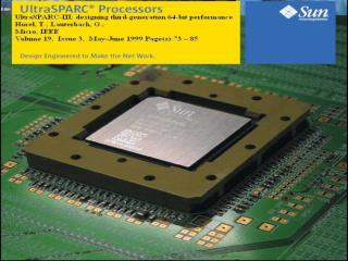
References [1] UltraSPARC-III: designing third-generation 64-bit performanceHorel, T.; Lauterbach, G.;Micro, IEEEVolume 19, Issue 3, May-June 1999 Page(s):73 – 85 [2] UltraSPARC-IV Processor Architecture Overview www.sun.com/processors [3] UltraSPARC Processors www.sun.com/ultrasparc [4] Throughput Computing www.sun.com/ultrasprac/throughput [5] Sun Microsystems http://en.wikipedia.org/wiki/Sun_Microsystems