Download
1 / 21
240 likes | 533 Views
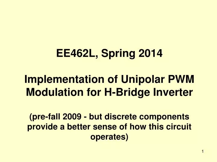
EE462L, Spring 2014 Implementation of Unipolar PWM Modulation for H-Bridge Inverter (pre-fall 2009 - but discrete components provide a better sense of how this circuit operates). Either A+ or A. –. is closed,. but never at th. e same time. Either B+ or B. –. is closed,.

E N D
EE462L, Spring 2014 Implementation of Unipolar PWM Modulation for H-Bridge Inverter (pre-fall 2009 - but discrete components provide a better sense of how this circuit operates)
Either A+ or A – is closed, but never at th e same time Either B+ or B – is closed, but never at the same time ! H-Bridge Inverter Basics – Creating AC from DC Switching rules Vdc A+ B+ Can use identical isolated firing signals for A+, A–, with inverting and non-inverting drivers to turn on, turn off simultaneously Va Vb Load Same idea for B+, B– A – B – The A+, A– firing signal is a scaled version of Va The B+, B– firing signal is a scaled version of Vb The difference in the two firing signals is a scaled version of Vab
! Vcont > Vtri , close switch A+, open switch A – , so voltage Va = Vdc Vcont < Vtri , open switch A+, close switch A – , so voltage Va = 0 – Vcont > Vtri , close switch B+, open switch B – , so voltage Vb = Vdc – Vcont < Vtri , open switch B+, close switch B – , so voltage Vb = 0 Implementation of Unipolar PWM Vcont is the input signal we want to amplify at the output of the inverter. Vcont is usually a sinewave, but it can also be a music signal. Vcont Vtri −Vcont The implementation rules are: Vtri is a triangle wave whose frequency is at least 30 times greater than Vcont. Ratio ma = peak of control signal divided by peak of triangle wave Ratio mf = frequency of triangle wave divided by frequency of control signal
! Vload Vdc −Vdc Implementation of Unipolar PWM Modulation for H-Bridge Inverter Progressivelywider pulses at the center (peak of sinusoid) Progressively narrower pulses at the edges Unipolar Pulse-Width Modulation (PWM)
! The four firing circuits do not have the same ground reference. Thus, the firing circuits require isolation. Vdc (source of power delivered to load) + + A B Local ground Local ground + + reference for A reference for B firing circuit firing circuit S S Load – – A B Local ground Local ground − − reference for A reference for B firing circuit firing circuit S S
Comparator Gives V(A+,A–) wrt. Common (0V) V(A+,A–) Vcont > Vtri +12V –12V Vcont < Vtri Use V(A+,A–) wrt. –12V Vcont > Vtri +24V 0V Vcont < Vtri Output of the Comparator Chip +12V from DC-DC chip 1.5kΩ 1.5kΩ 270kΩ Since the comparator compares signals that can be either positive or negative, the comparator must be powered by ±V supply Vtri Vcont 1kΩ 8 5 Comp 1 4 270kΩ –Vcont –12V from DC-DC chip Common (0V) from DC-DC chip
Comparator Gives V(B+,B–) wrt. Common (0V) V(B+,B–) –Vcont > Vtri +12V –12V – Vcont < Vtri Use V(B+,B–) wrt. –12V – Vcont > Vtri +24V 0V – Vcont < Vtri Output of the Comparator Chip +12V from DC-DC chip 1.5kΩ 1.5kΩ Since the comparator compares signals that can be either positive or negative, the comparator must be powered by ±V supply 270kΩ Vtri Vcont 1kΩ 8 5 Comp 1 4 270kΩ –Vcont –12V from DC-DC chip Common (0V) from DC-DC chip
+4V −4V 0V
+24V +24V 0V 0V
+24V +24V +24V +24V 0V 0V 0V 0V
+24V −24V 0V
+24V −24V +24V −24V 0V 0V Flat toping indicates the onset of overmodulation
+24V −24V 0V Approaching a square wave