Download
1 / 37
370 likes | 546 Views
A Low Mass On-chip Readout Scheme for Double-sided Silicon Strip Detectors. VCI 2013, 13 th Vienna Conference on Instrumentation. Outline. Introduction Assembly Cooling Summary. Motivation. Super KEKB Electron-positron collider 7 GeV e - on 4 GeV e +

E N D
A Low Mass On-chip Readout Scheme for Double-sided Silicon Strip Detectors C. Irmler, T. Bergauer, A. Frankenberger, M. Friedl, I. Gfall, A. Ishikawa, C. Joo, D.H. Kah, R. Kameswara, K.H. Kang, E. Kato, G. Mohanty, K. Negishi, Y. Onuki, N. Shimizu, T. Tsuboyama, S. Schmid, M. Valentan VCI 2013, 13th Vienna Conference on Instrumentation
Outline • Introduction • Assembly • Cooling • Summary VCI 2013, C. Irmler (HEPHY Vienna)
Motivation • Super KEKB • Electron-positroncollider • 7 GeV e- on 4 GeV e+ • Center of mass energy: Y(4S) (10.58 GeV) • Target luminosity: ~81035cm-2s-1 • Belle II detector • Refurbishment of all sub-detectors • 40 times higher luminosity • Faster readout Belle II Super KEKB ~1 km in diameter Linac About 60km northeast of Tokyo VCI 2013, C. Irmler (HEPHY Vienna)
Silicon vertex detector Belle (SVD2): • 4 layers of 4 inch DSSDs • Radii: 20 to 88 mm • Readout: VA1TA • 5 MHz / Tp = 800 ns • no pipeline • ENC = 180 e + 7.5 e/pF • Read out from edge of ladders • long pitch adapters • up to 3 ganged sensors Belle II SVD: • 4 layers of 6 inch DSSDs • Radii 38 to 135 mm • Readout: APV25 • 40 MHz / Tp= 50 ns • 192 cells analog pipeline • ENC = 250 e + 36 e/pF • Minimize capacitive load! • Chips closest to sensors strips chip-on-sensor • Keep material budget low VCI 2013, C. Irmler (HEPHY Vienna)
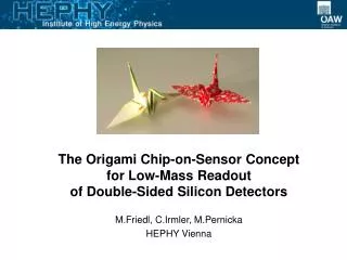
The Origami chip-on-sensor concept • CF reinforced ribs • 6” DSSD • 1mm Airex sheet • 3-layer flex circuit • Thinned APV25 (100µm) • Connection to Strips: • PA on top side • wrapped PA for bottom • Single cooling pipe • Trade-off between material budget & SNR • 0.55 X0 (averaged) n-side p-side VCI 2013, C. Irmler (HEPHY Vienna)
Belle II SVD Origami ladder • Exploded drawing of a L6 ladder • 3 different Origami flex designs • backward (-z), short tail • center (ce), for central sensor, long tail • forward (+z), routed along slanted sensor, complex shape VCI 2013, C. Irmler (HEPHY Vienna)
Outline • Introduction • Assembly • Cooling • Summary VCI 2013, C. Irmler (HEPHY Vienna)
The evolution of Origami modules • 2008: Introduction of concept • 2009: Feasibility shown with 4” DSSD module • 2010: First full-size module with 6” DSSD • 2011: Re-design to fit mechanical requirements of Belle II SVD ladders VCI 2013, C. Irmler (HEPHY Vienna)
Assembly of a 2-DSSD Origami module • How to assemble ladder withtwo or more Origami flexes? • Not possible sensor by sensor • Combined procedure required • 2-DSSD Origami module • 2 HPK DSSDs • Two types of Origami flexes (-z and ce) • Single-layer PA0/PA1/PA2 VCI 2013, C. Irmler (HEPHY Vienna)
Attaching of pitch adapters (PA1 & PA2) • Align PAs to p-side of sensor • Picked up with a vacuum jig • Apply mask and glue • Ensures uniform thickness • Future: cutting plotter • Place back onto sensor • Curing of glue VCI 2013, C. Irmler (HEPHY Vienna)
Attaching Origami flexes • Wire bonding p-side • Placing sensors onto an assembly bench • Optical alignment (not done this time) • Attaching Airex sheets(in future: 1 per ladder) • Glue Origami PCBs • pre-assembled APV chips • first CE • then –z • Wire bonding n-side -z CE VCI 2013, C. Irmler (HEPHY Vienna)
Bend and glue PA1, PA2 • PA1 & PA2 have to be bent toward top side • Micro positioner with vacuum head • Apply glue using masks • Pre-bend PA and align vacuum head • Align PA to APV and lower down • Glue curing • Followed by ~2500 wire bonds Custom vacuum nozzle VCI 2013, C. Irmler (HEPHY Vienna)
Attaching CF ribs • Mount ribs on jig • Place rib jig onto assembly bench • Dispense glue • Place sensors onto ribs • Distance given by precise spacers • Cure glue • Remove spacers and lower down assembly bench VCI 2013, C. Irmler (HEPHY Vienna)
Outline • Introduction • Assembly • Cooling • Summary VCI 2013, C. Irmler (HEPHY Vienna)
Cooling of Origami APV chips • ~10 W per ladder • Efficient CO2 cooling • Single cooling pipe for several ladders • Little space for connections • Outer 1.6 mm • Custom fixture to hold the pipe Cooling pipe VCI 2013, C. Irmler (HEPHY Vienna)
Cooling contact requirements • Re-mountable cooling pipe (no glue …) • Easy and safe mounting (bond wires …) • Avoid stress at sensor (thermal expansion) • Efficient heat transfer • large contact area • compensate height differences of APVs • thermally conductive gap pads • Electrically isolating • Radiation hard material VCI 2013, C. Irmler (HEPHY Vienna)
Thermallyconductivegap pad • Heatload/APV: 0.35W • Coolanttemperature: -20°C • Tube: • stainlesssteel AISI 316L • wall thickness100μm • Gap pad: 86/125 Keratherm • λ [W/mK]: 1.5W/mK • Very soft, 1mm thick • Radiation hardness wastestedin October 2012 VCI 2013, C. Irmler (HEPHY Vienna)
Pipe clamp Hinge clamp: • PEEK G450 • micro water jet cutting • fabrication tolerance: 0.01 mm • Max. wall thickness: 20 mm • Min. inner radius: 0.1 mm • Disadvantage: 2 parts • Prototypes tested on 2-DSSD module VCI 2013, C. Irmler (HEPHY Vienna)
Cooling pipe mounting • Clamp bases glued onto Origami PCB • Keratherm strips placed onto APV chips • Pipe put into camp bases • Clamps closed VCI 2013, C. Irmler (HEPHY Vienna)
Final Module with cooling pipe VCI 2013, C. Irmler (HEPHY Vienna)
Improved version of clamp • Material: PEEK • Improved shape • Single part • Clamp force: ~3 N • Prototypes tested on dummy • Works well • Easy to assemble VCI 2013, C. Irmler (HEPHY Vienna)
Performance of CO2 cooling • Temperature measured at 4 locations of the 2-DSSD module • Stable operation for ~18 hours • Nominal temperature: -20°C • All temperatures within precision of probes no warming of coolant • Efficient heat transfer between chips and pipe (coolant) Temperatur [°C] Module Inlet Module Outlet Origami –z Origami ce Time VCI 2013, C. Irmler (HEPHY Vienna)
Beam test performance • Beam test performed @ CERN SPS in October 2012 • 120 GeV/c (mainly pions) • Module operated with CO2 cooling at -20 °C • Signal-to-noise ratio: • Many noisy channels due to wire bonding problems (new wire bonder) • Origami –z performed well (compared to single-sensor modules) • Origami ce suffered from noisy channels VCI 2013, C. Irmler (HEPHY Vienna)
Outline • Introduction • Assembly • Cooling • Summary VCI 2013, C. Irmler (HEPHY Vienna)
Summary • Origami chip-on-sensor concept • A low mass on-chip readout for 6” DSSD (0.55 X0avg.) • Feasibility proven by several prototypes • Will be utilized for the Belle II SVD • Assembly procedure shown for a 2-DSSD module • Two-phase CO2Cooling: • Single tube for several ladders • Design and prototypes of tube clamp available • Beam test @ CERN in October 2012 • Ladder production scheduled for autumn 2013! VCI 2013, C. Irmler (HEPHY Vienna)
Thank You VCI 2013, C. Irmler (HEPHY Vienna)
Backup Slides VCI 2013, C. Irmler (HEPHY Vienna)
Belle II SVD Sensor underneath flex circuit End ring (support) APV25 chips Origami ladder Pitch adapter bentaround sensor edge Cooling pipe VCI 2013, C. Irmler (HEPHY Vienna)
Team K. Kamesh (TIFR), C. Irmler (HEPHY), Y. Onuki (Tokyo U.), K. Negishi (Tohoku U.) N. Shimizu (Tokyo U.) E. Kato (Tohoku U.) VCI 2013, C. Irmler (HEPHY Vienna)
Origami PCBs 3 types of 3-layer Origami PCBs: • backward (-z), short tail • center (ce), for central sensor, long tail • forward (+z), routed along slanted sensor, complex shape -z ce +z VCI 2013, C. Irmler (HEPHY Vienna)
Pitch Adapters • All available in single- and double-layer designs • PA0: short, n-side, glued onto Origami PCB • PA1: first half of p-side strips • PA2: second half of p-side strips Bond pads of single-layer PAs VCI 2013, C. Irmler (HEPHY Vienna)
Attaching Airex 1 • We used one piece per sensor • Later we will use a single sheet per ladder 2 4 3 VCI 2013, C. Irmler (HEPHY Vienna)
Attaching Origami hybrids • Aligned CE to sensor • Lifted it with Origami jig • Applied glue • Put back onto assembly bench • Waited until glue has been cured • Removed Origami jig • Aligned –z to sensor • Repeated from step 2. VCI 2013, C. Irmler (HEPHY Vienna)
Attaching Origami CE 1 2 4 3 5 VCI 2013, C. Irmler (HEPHY Vienna)
Attaching Origami -z VCI 2013, C. Irmler (HEPHY Vienna)
Bend and Glue PA1, PA2 – Apply Mask 3: dispense glue 1: apply mask 4: flatten glue 5: remove mask 2 VCI 2013, C. Irmler (HEPHY Vienna)
Final Module in Frame Top and bottom views (w/o cooling pipe) VCI 2013, C. Irmler (HEPHY Vienna)