Download
1 / 26
270 likes | 455 Views
Silicon Strip Readout and the XYTER Electronics Development. Christian J. Schmidt et al., GSI Darmstadt. 10th CBM Collaboration Meeting, Dresden, Sept. 24. – 28., 2007. Challenging Experiments, Challenging Detector Specs.

E N D
Silicon Strip Readoutand the XYTER Electronics Development Christian J. Schmidt et al., GSI Darmstadt 10th CBM Collaboration Meeting, Dresden, Sept. 24. – 28., 2007
Challenging Experiments, Challenging Detector Specs • As a fixed target machine, very high event-rates (1000 tracks at 10MHz for CBM) • Up to 5% channel occupancy, • Very inhomogeneous track distribution (forward cone) • Signal latency will be too large for a timely, reasonable trigger decision, • Event overlap expected Need front-end electronics: MIPs at high input capacitance highly integrated, asynchronous, autonomous hit detection, time stamp labeling.
Additionally • Very harsh radiation environment (10 MRad) • Very high density channels with need for either • low radiation-length detector design (CBM-STS, PANDA TPC, PANDA forward GEM trackers, CBM TRD) ... or • very compact detector design (e.g. CBM-Muon Chambers)
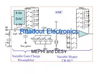
n-XYTER: Novel FE-Chip Architecture Cast in Silicon Architectural Solution for FAIR CBM and PANDA. Starting point towards a FAIR dedicated XYTER front-end ASIC Our work-horse readout ASIC for detector prototyping detector readout ASIC for high-density and high statistical rate time and amplitude measurement • 128 channels @ 50.7 µ pitch • freely running, self triggered autonomous hit detection • 850 (1000) ENC at 30 pF • dynamic range for 6 MIPs (300µ Si) • positive and negative signals • Per channel analogue energy and digital time stamp FIFO (1ns resolution) • De-randomizing, sparsifying Token Ring readout at 32 MHz n-XYTER was developed for neutron applications within EU FP-6 NMI3
Data Driven Front-End: Asynchronous Channel Trigger detection of statistical, poisson distributed signals triggertimestamp reg. comparator Time WalkCompensationcircuit FASTshaper 18.5 ns peaking PDH reset chargepreamp dig. FIFO chargeinput SLOW shaper(2 stages) 140 ns peaking time Peakdetector & hold, free running pulse height output analogue FIFO Asynchronous registry and storage in 4-level fifo guarantees data loss < 4 % when read-out through token ring The DETNI ASIC 1.0, a front-end evaluation chip in AMS 0.35µ
Analogue Signal Sequence (Test Channel) Testpulse Release Slow Shaper Fast Shaper Discriminator Output
Test Board for Tests on n-XYTER • 64/128 chan. connected • I²C-Interface • Test points accessible • All functional tests possible • Digital output accessible One additional analogue test channel is available for direct access of slow and fast shaper outputs...with output buffer would have been even more useful
FAST channel SLOW channel ENC 26.9 e/pF + 200 e 12.7 e/pF + 233 e peaking timea (1% to 99%) 18.5 ns 139 ns Analogue Pulses, Peaking Time, Front-End Noise Engineered for 30 pF, giving (850 ) 1000 e 600 e pre-amp and shaper power consumption: 12.8 mW per channel; OK for neutrons!
Slow Shaper Output, the Energy Channel Measurements on the test channel #129 varying input capacitance varying input charge
Some Inter-Channel Pick-Up, Ongoing Detective Work Cin = 0 pF, bond wire removed Cin = 22 pF • System Effect • No dependence upon no. of bond wires, power or gnd • May be worsened with discriminator settings (TWC) Feedback via spurious coupling through epitaxial, optical layer, substrate to the input
Some In-Channel Discriminator Feedback Detected ...upon removal of discriminator-power decoupling correlates with internal discriminator trigger correlates with external test-pulse release signal (blue) These issues are particularly important with the self triggered architecture! They will be addressed even more in the next engineering run.
Channel layout overview, Clock Domains and Power time stampfast clock analogue domain no clock digital domain system clock total of 4 nF on chip MIM caps memory control ( 9 bit ) PDH reset comp analogue front end , PDH comp – TWCtrim reg analoguemem. maskreg. mono synch control tokencell ch.ID digitalmem. TSlatch clocktree PAD A/Dguard ring input MOSGND digitalBULK analogueGND& BULK analogueVDD comparatorVDD digitalGND digitalVDD 8 mm 5 mm
Token Ring Readout, Data Transmission DataValid Measurement: Transmission of four data elements on channels 1, 8, 30, 82 TS grey coded Ch# grey coded data transfer tested at 35 MHz, will also work at 128 MHz
Analogue Differential Output, the Energy Channel Three signals, one signal altered Signal settling upon successive data
Power Consumption • preamplifier 7.4mW • fast shaper 2.5mW • slow shaper stage 1 1.7 mW • slow shaper stage 2 2.5 mW • discriminator 2.1 mW • peak detector and hold 2.7 mW • analogue FIFO 2.3 mW overall we find 21 mW/channel operating power
Testing Summary Testers involved: Gerd Modzel (PI HD) Markus Höhl (GSI) Knut Solvag (GSI) Sharma Anurag (Dehli) Rafal Lalik (AGH, GSI) Adam Czermak (AGH) thanks for his support to Sven Loechner (GSI) and others • Slow Control Operative • Clocking at 256 MHz possible • Grey coded time stamp generated • Analogue readout operative • Features operative: • Positive and negative signal processing • Global threshold, local threshold fine tune • On chip test pulse generation • Channel masking • Channel forced trigger (baseline determination) • Individual channel shut down • Pile-up lableing, fifo overflow identification
n-XYTER Engineering Run in Preparation From 250 Dies to Work Horse Electronics for Detector Prototyping • Engineering Run Targeted for Jan. 2008 H. K. Soltveit (PI Heidelberg) • Addresses active feedback baseline adjustment full dynamic range, no temp. co. on base-line • Addresses spurious feedback coupling through substrate • Reduction of power consumption where easily possible Will yield several thousand chips for prototyping of CBM STS, PANDA TPC and other detectors as well as the DAQ chain and beyond. Go Detector Prototyping
Dedicated XYTER Development for FAIR Generic n-XYTER architecture finds broad applications within FAIR: CBM Silicon Strips STS, High Rate GEM TPC as well as large area gas detectors (micro structures or wire chambers) Twin chip development with XYTER architecture and diversities for: Silicon Strip MIP detection, micro-structured gas detectors Larger dynamic range, ion tail cancellation specialties • Radiation hard design in UMC 0,180 µm (better than 10 MRad) • Minimized power consumption • Integration of modern, low power ADC on chip purely digital interface • Highly multiplexed data interface (minimize cableing) • Optimized system synchronization capabilities • SEU tolerance • Detector DC coupling capability • Dense mounting capability
CBM Groups Involved In XYTER Development • AGH Krakow, (Robert Szczygiel, Pawel Grybos et al.) • TI Heidelberg (Peter Fischer and Tim Armbruster) • MEPHI, Moscow (E. Atkin et al) • PI Heidelberg and HD ASIC-Lab (H. K. Soltveit) • GSI Darmstadt, C.J. Schmidt (coordination) and Sven Loechner Further engaged: • S. Chattopadhyay et al, Kolkatta on individual design items • University Bergen, K. Ulaland and D. Röhrig et al We will structure the XYTER development collaboration Friday morning 9:00 to 11:00
CBM Thank you for your attention
Token Ring Architectural Pros/Cons • High Efficiency • Empty channels automatically skipped in readout process • Built-in fair distribution of readout bandwidth, automatic bandwidth focussing • Built-in De-Randomization: 100% bandwidth used on data • Error Robustness • Any problematic channel (e.g. continuously firering) will divert and occupy a maximum of 1/nth of the bandwidth. • Built-in, non-perfect readout probability avoids unrecoverable logic deadlock: Problematic situations like any kind of pile-up, logic hang-ups or glitch cause mere deadtime but the “show will go on”. But: Data needs to be tagged with a time-stamp Data needs to be resorted and re-bunched after readout
Investigating Individual Channels, Triggerefficiency Trigger efficiency in Treshold Scan: The S-Curves Derivative gives image of noise! - Input of test pulses at fixed rate, - scan threshold while measuring detection rate
Trigger efficiency tested for all channels Channel number note bonded and non-bonded channels origin of 2 ch periodicity attributed to four fold pulser circuitry
Token Ring Readout Process token cycle token cell control logic for data readout or token pass Analog FIFO Disc. Timestamp FIFO data readout bus skip channels without data, asynchronously rush through empty channels until data found • Focus bandwidth where there is data • 32 MHz data readout • Automatic zero suppression (sparsification)
1 2 3 4 5 6 7 8 9 10 11 12 13 0.2 0.15 Probability 0.1 We loose from here on 0.05 0 0 1 2 3 4 5 6 7 8 9 10 11 12 Modelling FIFO Occupancy Poisson Distribution(l): e.g.: fifo depth n = 4, so expect 4 events during readout if incoming rate equals maximum readout rate. l = 4. FIFO can virtually be filled with up to 2*n events with no data loss since n elements are read while data comes in.