Download
1 / 43
440 likes | 764 Views
Learn about semiconductor physics including n and p-type silicon, dopant contributions in doped Si, pn junctions, built-in voltage, forward and reverse bias effects, and BJT operations in active, saturation, and cutoff modes.

E N D
Semiconductor Physics & Bipolar Junction Transistor (BJT)
n- and p-type silicon • Pure silicon is an insulator. At high temperatures it conducts weakly. • If we add an impurity with extra electrons (e.g. arsenic, phosphorus) these extra electrons are set free and we have a good conductor (n-type silicon). • If we add an impurity with a deficit of electrons (e.g. boron) then bonding electrons are missing (holes), and the resulting holes can move around and will make good conductor (p-type silicon)
Intrinsic (undoped) Si N-doped Si Assume each dopant contribute to one electron P-doped Si Assume each dopant contribute to one hole Electron and Hole Densities in Doped Si
The pn Junction Schematic diagram • p-n junctions form the essential basis of all semiconductor devices • A silicon chip may have 108 to109 p-n junctions. p-type n-type net donor concentration ND net acceptor concentration NA cross-sectional area AD Physical structure metal SiO2 SiO2 p-type Si For simplicity, assume that the doping profile changes abruptly at the junction. n-type Si metal
– – – – – Depletion Region • When the junction is first formed, mobile carriers diffuse across the junction (due to the concentration gradients) Holes diffuse from the p side to the n side, leaving behind negatively charged immobile acceptor ions Electrons diffuse from the n side to the p side, leaving behind positively charged immobile donor ions • The space charge due to immobile ions in the depletion region establishes an electric field that opposes carrier diffusion. acceptor ions donor ions + A region depleted of mobile carriers is formed at the junction. + pn + + + depletion region This potential difference is called the built-in voltage and is given by: • There are essentially no mobile electrons or holes in this region, and because of the electric field in the depletion region, there will be a potential difference across that region.
The Depletion Capacitance (Junction Capacitance) • For a pn junction under reverse biased condition ,due to the additional positive and negative charges in the depletion region, and an increase in reverse-bias voltage, a capacitance is associated. • is the junction capacitance with zero voltage applied • is the applied reverse voltage across the diode • is the built-in voltage
Forward biased diffusion capacitance, CD • CD is also called the charge storage capacitance. The variation of the injected minority-carrier charge, which is a function of the applied bias, results in the diffusion capacitance. Both CJ and CD are always present, but for the forward-bias case, CD becomes dominant. p-type n-type np0 pn0 For a pn junction, I = Qp/p , where Qp is total excess charge in p-side Where, Ip >>In And Lp = Excess-minority-carrier lifetime
– – – – – Forward Bias Effect of Applied Voltage • As VD increases, the potential barrier to carrier diffusion across the junction decreases*, and current increases exponentially. The carriers that diffuse across the junction become minority carriers in the quasi-neutral regions; they then recombine with majority carriers, “dying out” with distance. + VD > 0 + pn + + + The depletion region has high resistivity. Thus almost all of this voltage is dropped across the depletion region. ID (Amperes) VD (Volts) * Hence, the width of the depletion region decreases.
– – – – – Reverse Bias Effect of Applied Voltage(Cont’d) • As |VD| increases, the potential barrier to carrier diffusion across the junction increases*; thus, no carriers diffuse across the junction. A very small amount of reverse current (ID < 0) does flow, due to minority carriers diffusing from the quasi-neutral regions into the depletion region and drifting across the junction. + VD < 0 + pn + + + ID (Amperes) VD (Volts) * Hence, the width of the depletion region increases.
Terminals & Operations • Active: • Most important mode, e.g. for amplifier operation and switching application • The region where current curves are practically flat. • Saturation: • Barrier potential of the junctions cancel each other out causing a virtual short. • Ideal transistor behaves like a closed switch. • Cutoff: • Current reduced to zero • Ideal transistor behaves like an open switch.
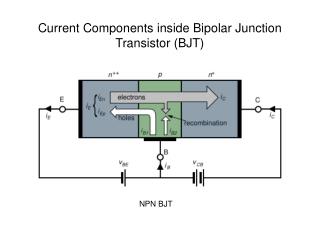
BJT in Active Mode • Operation • Forward bias of EBJ injects electrons from emitter into base (small number of holes injected from base into emitter) • Most electrons shoot through the base into the collector across the reverse bias junction • Some electrons recombine with majority carrier in (P-type) base region
Profiles of minority-carrier concentration Current dominated by electrons from emitter to base , b/c of the forward bias and minority carrier concentration gradient (diffusion) through the base • Diffusion of electrons through the base is set by concentration profile at the EBJ • Diffusion current of electrons through the base is (assuming an ideal straight line case): • Due to recombination in the base, the current at the EBJ and current at the CBJ are not equal and differ by a base current
Collector Current • Most of the diffusing electrons will reach the boundary of the collector-base depletion region. Because the collector is more positive than the base (by vCB) , these electrons will be swept across the CBJ depletion in to the collector . • Note that iC is independent of vCB(potential bias across CBJ) ideally • Saturation current is inversely proportional to W and directly proportional to AE • Want short base and large emitter area for high currents
Base Current • Base current iB composed of two components: • holes injected from the base region into the emitter region • holes supplied by the external circuit in order to replace the holes lost from the base through the recombination process . And the Qn in the base is So, current is • Total base current is • iB can be expressed as a fraction of iCas. • Where ,
Emitter Current • Emitter current is the sum of iC and iB a is called the common-base current gain
Large-Signal Model For BJT (Ebers-Moll Model ISC and ISE are the scale or saturation currents of diodes DE (EBJ) and DC (CBJ). Terminal Currents can be derived as :
Characteristics of Bipolar Transistor The collector is constant current source only controlled by emitter current IE
Early Effect • The Early Effect • The collector current in active region depends (slightly) on vCE • VA is a parameter for the BJT and called the Early voltage • Due to a decrease in effective base width W as reverse bias increases • Account for Early effect with additional term in collector current equation • Nonzero slope the ic-vCEindicates the output resistance is NOT infinite, but finite and defined by
Hybrid-Pi Model of BJT Transconductance: Input resistance: • The hybrid-pi small-signal model is the intrinsic representation of the BJT. • Small-signal parameters are controlled by the Q-point and are independent of geometry of the BJT Output resistance:
BJT frequency Response • As the frequency of the processed signals increases, the effects of parasitic capacitance in BJT transistors start to manifest • The gain of the amplifier circuits is frequency dependent, usually decrease with the frequency increase of the input signals
The Base-Charging or Diffusion Capacitance • When the transistor is operating in the active or saturation modes , minority-carrier charge is stored in the base region , this charge - storage mechanism represents a nonlinear capacitive effect . • Diffusion capacitance almost entirely exists in forward-biased pn junction • Expression of the small-signal diffusion capacitance • Proportional to the biased current
Junction Capacitances Due to the additional positive and negative charges in the depletion region, and increase in reverse-bias voltage, a capacitance is associated. • The Base-Emitter Junction Capacitance • The collector-base junction capacitance
The High-Frequency Gain Function • The transfer function of a circuit can be written in the general form • Rules for generating a Bode magnitude vs. frequency plot: • - As ω passes each zero frequency, the slope of |H(jω)| increases by 20dB/dec. • - As ω passes each pole frequency, the slope of |H(jω)| decreases by 20dB/dec.
Short-circuit current gain. The High-Frequency hybrid- Model Where, The current , from KCL is Nodal equation of the B node: Hence, from these equations we can get
The Cutoff and Unity-Gain Frequency The 3dB-frequency Unity-Gain Bandwidth We can find fT (unity current gain frequency) by setting |β(jωΤ)| = 1.
Miller’s Theorem In the analysis of high-frequency response we can replace the bridging capacitance Cµ by an equivalent input capacitance . Due to Miller effect, a small feedback capacitance that appears across the input terminals has a much larger equivalent capacitance with a large gain. At high frequencies, this large capacitance has a low impedance that tends to short out the input signal Impedance Z can be replaced by two impedances: Z1 connected between node 1 and ground Z2 connected between node 2 and ground For the Miller replacement ,if the feedback element is a capacitance its value is multiplied by (1-k) to obtain the equivalent capacitance at the input side , this multiplication is referred to as Miller Effect
The Frequency Bands Consider the Capacitively coupled Common - Emitter amplifier shown below Sketch of the magnitude of the gain of the CE amplifier versus frequency. The graph delineates the three frequency bands relevant to frequency-response determination.
The High-Frequency Response of CE Amplifier • At high frequency the coupling capacitors and the bypass capacitor will be behaving as a perfect short circuits Simplified circuit by utilizing Thevenin theorem at the input side and by combining the three resistances at output side
(cont’d) The High-Frequency Response • Using Miller’s theorem Equivalent circuit with replaced at the input side with the equivalent capacitance ; Hence, the total capacitance from terminal B’ to ground is given as follows Using these equations the voltage gain in the high frequency band can be derived as The frequency response plot From which the upper 3-dB frequency fH must be
The BJT Cascode Stage • A cascode stage has high output impedance, which is advantageous for Achieving high voltage gain Use as a current source • the cascode amplifier can be designed to obtain a wider band width but equal dc gain as compared to the common–emitter amplifier ,Alternatively it can be designed to increase the dc gain while leaving the gain-bandwidth product unchanged • In a cascode stage, the Miller effect is reduced, that improve performance at high frequencies.
The BJT Cascode Amplifier The cascode with the output open-circuited with gain at different stage indicated The circuit prepared for small-signal analysis with various input and output resistances indicated. Note that , rx is neglected
The BJT Cascode (Cont’d) Equivalent circuit in terms of the overall short-circuit transconductance Gm =gm. Equivalent circuit for the cascode amplifier in terms of the open-circuit voltage gain Avo = –bA0 Equivalent circuit for determining the gain of the CE stage, Q1.
Frequency Response of the BJT Cascode Open Circuit time constant Note that in addition to the BJT capacitances Cp and Cm, the capacitance between the collector and the substrate Ccs for each transistor are also included.
The BJT Current-Mirror A current mirror is used to replicate the current from a “golden current source” to other locations. Analysis of the current mirror taking into account the finite b of the BJTs. Q1 and Q2 are matched and have the same VBE , their collector current will be equal Since Io = Ic , the current transfer ratio can be found us
The BJT Current-Mirror(Cont’d) The Wilson bipolar current mirror showing current transfer ratio Circuit to determining the output resistance. Note that the current ix that enters Q3 must equal the sum of the currents that leave it, 2i.
BJT Differential Pair Denote the voltage at the common emitter by VE Large-Signal Operation Combining these equations And, Which gives The basic BJT differential-pair configuration.
BJT Differential Pair (Cont’d) A relatively small difference voltage Vid will cause the current I to flow almost entirely in one of the two transistors ,such a small signal can switch the current from one side of the BJT differential pair to the other ,means that the BJT differential pair can be used as a fast current switch . Transfer characteristics of the BJT differential pair assuming a =1
Small-Signal Operation Multiplying the numerator and denominator by The incremental current component ic is given by The currents and voltages in the differential amplifier when a small differential input signal vid is applied. And , Where,
Differential Pair Frequency Response Since the differential pair can be analyzed using its half circuit, its transfer function, I/O impedances, locations of poles/zeros are the same as that of its half circuit.
References : • Microelectronic Circuits by Adel S.Sedra and kenneth C.Smith(fifth edition) • http://www.educypedia.be/electronics/analogmisac.htm • http://inst.eecs.berkeley.edu/~ee40/fa07/lectures/