Chapter 5 pn Junction Electrostatics
Semiconductor Device Physics. Chapter 5 pn Junction Electrostatics. Chapter 5. pn Junction Electrostatics. Metallurgical Junction. Doping profile. Step junction idealization. Chapter 5. pn Junction Electrostatics. Poisson’s Equation.


Chapter 5 pn Junction Electrostatics
E N D
Presentation Transcript
Semiconductor Device Physics Chapter 5 pn Junction Electrostatics
Chapter 5 pn Junction Electrostatics Metallurgical Junction • Doping profile Step junction idealization
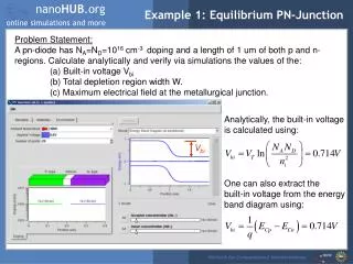
Chapter 5 pn Junction Electrostatics Poisson’s Equation • Poisson’s equation is a well-known relationship in electricity and magnetism. • It is now used because it often containsthe starting point in obtaining quantitative solutions for the electrostatic variables. • In one-dimensional problems, Poisson’s equation simplifies to:
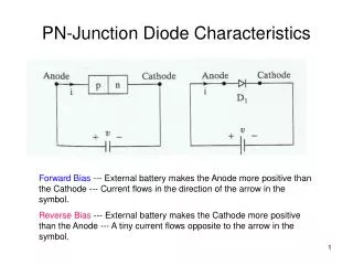
Chapter 5 pn Junction Electrostatics Equilibrium Energy Band Diagram • pn-Junction diode
Chapter 5 pn Junction Electrostatics Qualitative Electrostatics • Equilibrium condition Band diagram Electrostatic potential
Chapter 5 pn Junction Electrostatics Qualitative Electrostatics • Equilibrium condition Electric field Charge density
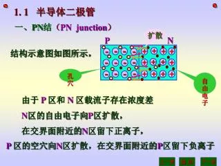
Chapter 5 pn Junction Electrostatics Formation of pn Junction and Charge Distribution – + qNA qND
Chapter 5 pn Junction Electrostatics Formation of pn Junction and Charge Distribution
Chapter 5 pn Junction Electrostatics Built-In Potential Vbi • Vbi for several materials: • Ge ≤ 0.66 V • Si ≤ 1.12 V • GeAs ≤ 1.42 V • For non-degenerately doped material,
Chapter 5 pn Junction Electrostatics The Depletion Approximation • On the p-side,ρ = –qNA with boundary E(–xp) = 0 • On the n-side,ρ = qND with boundary E(xn) = 0
Chapter 5 pn Junction Electrostatics Step Junction with VA=0 • Solution for ρ • Solution for E • Solution for V
Chapter 5 pn Junction Electrostatics Relation between ρ(x),E(x),and V(x) • Find the profile of the built-in potential Vbi • Use the depletion approximation ρ(x) • With depletion-layer widths xp, xn unknown • Integrate ρ(x) to find E(x) • Boundary conditionsE(–xp) = 0, E(xn)=0 • Integrate E(x) to obtain V(x) • Boundary conditions V(–xp) = 0, V(xn) =Vbi • For E(x) to be continuous at x = 0, NAxp =NDxn • Solve for xp, xn
Chapter 5 pn Junction Electrostatics Step Junction with VA=0 • At x = 0, expressions for p-side and n-side for the solutions of E and V must be equal:
Chapter 5 pn Junction Electrostatics Depletion Layer Width • Eliminating xp, • Eliminating xn, Exact solution, try to derive • Summing
Chapter 5 pn Junction Electrostatics One-Sided Junctions • If NA>>NDas in a p+njunction, • If ND>> NAas in a n+pjunction, • Simplifying, • where N denotes the lighter dopant density
Chapter 5 pn Junction Electrostatics Example: Depletion Layer Width • A p+n junction has NA = 1020 cm–3 and ND = 1017cm–3, at 300 K. • a) What isVbi? • b) What is W? • c) What is xn? • d) What is xp?
Chapter 5 pn Junction Electrostatics Step Junction with VA 0 • To ensure low-level injection conditions, reasonable current levels must be maintained VA should be small
Chapter 5 pn Junction Electrostatics Step Junction with VA 0 • In the quasineutral, regions extending from the contacts to the edges of the depletion region, minority carrier diffusion equations can be applied since E ≈ 0. • In the depletion region, the continuity equations are applied.
Chapter 5 pn Junction Electrostatics Step Junction with VA 0 • Built-in potential Vbi (non-degenerate doping): • Depletion width W :
Chapter 5 pn Junction Electrostatics Effect of Bias on Electrostatics • If voltage dropâ,thendepletion width â • If voltage drop á, then depletion width á
Chapter 5 pn Junction Electrostatics Linearly-Graded Junction
Chapter 5 pn Junction Electrostatics Homework 4 • 1. (6.4) • Consider a silicon pn junction at T = 300 K with a p-side doping concentration of NA= 1018 cm–3. Determine the n-side doping concentration such that the maximum electric field is |Emax| = 3×10⁵ V/cm at a reverse bias voltage of VR= 25 V. • 2. (7.6) • Problem 5.4Pierret’s “Semiconductor Device Fundamentals”. • Due: 17.09.2013.