Bipolar Junction Transistors (BJTs)
230 likes | 567 Views
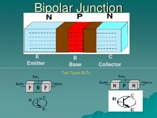
Bipolar Junction Transistors (BJTs). The bipolar junction transistor is a semiconductor device constructed with three doped regions . These regions essentially form two ‘back-to-back’ p-n junctions in the same block of semiconductor material (silicon).

Bipolar Junction Transistors (BJTs)
E N D
Presentation Transcript
Bipolar Junction Transistors (BJTs) • The bipolar junction transistor is a semiconductor device constructed with three doped regions. • These regions essentially form two ‘back-to-back’ p-n junctions in the same block of semiconductor material (silicon). • The most common use of the BJT is in linear amplifier circuits (linear means that the output is proportional to input). It can also be used as a switch (in, for example, logic circuits).
p-type n-type n-type npn-BJT Structure • The ‘npn’ version of the BJT consists of two n regions separated by a p region (as the name suggests). A schematic of an npn transistor is shown.
BJT Structure • The three regions are known as the emitter, base and collector regions. • Electrical connections are made to each of these regions.
E Base (p-type) C Emitter (n-type) Collector (n-type) B npn-BJT Structure
C B E npn BJT Symbol
C B E pnp BJT Symbol • In the symbol for a pnp BJT transistor the direction of the arrow on the emitter is reversed
BJT Circuits • Most electronic devices take the signal between two input terminals and deliver from it an output signal between two output terminals. • The BJT has only three terminals so one of these is usually shared (i.e. made common) between input and output circuits. • We thus talk about common emitter (CE), common base (CB) and common collector (CC) configurations.
BJT Circuits • The CE configuration is the one most commonly encountered since it provides both good current and voltage gain for ac signals. • In the CE configuration the input is between the base and the emitter. The output is between the collector and the emitter. • All three configurations will be covered in the module lectures.
Current Directions (Convention) • We define currents directions such that the collector current (IC) and base current (IB) flow into the device whereas the emitter current (IE) flows out of the device. • THIS IS IMPORTANT; we shall shortly treat the transistor as a current node and write IC + IB = IE (Kirchhoff)
E Base (p-type) C Emitter (n-type) Collector (n-type) B Current Flow Convention IE IC IB
npn BJT Structure • The emitter (E) and is heavily doped (n-type). • The collector (C) is also doped n-type. • The base (B) is lightly doped with opposite type to the emitter and collector (i.e. p-type in the npn transistor). • The base is physically very thin for reasons described below.
B-E and C-B Junctions • The p-n junction joining the base and emitter regions is called the base-emitter (B-E) junction. (or emitter-base, it doesn’t really matter) • The p-n junction between the base and collector regions is called the collector-base (C-B) junction.(or base-collector)
(Very) Basic Operation • In normal operation for analogue (linear amplifier) circuits the emitter-base junction is forward biased and the collector-base junction is reverse biased. • These ‘bias’ or ‘quiescent’ conditions are set by d.c. bias circuits. • The a.c. (‘analogue’) signal to be amplified is superimposed on top of the d.c. bias voltages and currents. (Exactly as for dynamic resistance, small variations about a Q point, in our discussion of diodes.)
B (p) E (n) C (n) E C B BJT Operation • The forward bias between the base and emitter injects electrons from the emitter into the base and holes from the base into the emitter.
BJT Operation • The forward bias between the base and emitter injects electrons from the emitter into the base and holes from the base into the emitter. • As the emitter is heavily doped and the base lightly doped most of the current transport across this junction is due to the electrons flowing from emitter to base.
BJT Operation • The base is lightly doped and physically very thin. • Thus only a small percentage of electrons flowing across the base-emitter (BE) junction combine with the available holes in this region.
BJT Operation • Most of the electrons (a fraction α which is close to 1, e.g. 0.98) flowing from the emitter into the base reach the collector-base (CB) junction. • Once they reach this junction they are ‘pulled’ across the reverse biased CB junction into the collector region i.e. they are collected. • Those electrons that do recombine in the base give rise to the small base current IB.
BJT Operation • The electrons ‘collected’ by the collector at the C-B junction essentially form the collector current in the external circuit. • There will also be a small contribution to collector current, called ICO,from the reverse saturation current across the CB junction. • The base current supplies positive charge to neutralise the (relatively few) electrons recombining in the base. This prevents the build up of charge which would hinder current flow.
BJT Operation.The Critical Knowledge! • The (relatively large) collector current is directly controlled by the (much smaller) base current. • This is further illustrated and clarified in the following discussions of the BJT’s current-voltage characteristics.
BJT Transistor Man (after Horowitz and Hill) βIB Forward biased diode