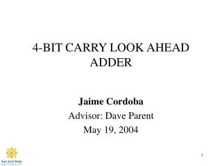
4-BIT CARRY LOOK AHEAD ADDER
4-BIT CARRY LOOK AHEAD ADDER. Jaime Cordoba Advisor: Dave Parent May 19, 2004. Agenda. Abstract Introduction Why Simple Theory Back Ground information (Lit Review) Summary of Results Project (Experimental) Details Results Cost Analysis Conclusions. Abstract.

4-BIT CARRY LOOK AHEAD ADDER
E N D
Presentation Transcript
4-BIT CARRY LOOK AHEAD ADDER Jaime Cordoba Advisor: Dave Parent May 19, 2004
Agenda • Abstract • Introduction • Why • Simple Theory • Back Ground information (Lit Review) • Summary of Results • Project (Experimental) Details • Results • Cost Analysis • Conclusions
Abstract • I designed an 4-bit carry look ahead adder that operates at a frequency of 200 MHz and has a propagation delay of .5ns and occupies an area of 375 x 160mm^2
Introduction • Carry look ahead adders are important because they are building blocks for other logics such as MSI adders and ALUs. • The carry look ahead logic is the adder stage that generates a carry and propagates carry
Project Details • Hand Calculations • Cell based technique • Build each layout of gate seperately and performed an LVS • Final Schematic • Final Layout • Final Simulation
Longest Path Calculations Note: All widths are in microns and capacitances in fF
Cost Analysis • Time spent on each phase of project • verifying logic= 10 hours • verifying timing= 5 hours • Layout= 25 hours • post extracted timing= 5 hours
Lessons Learned • Do not procrastinate • Start as early as possible • Make a schedule and follow it • Talk to your instructor
Summary • My objective was to design a 4-bit carry look ahead adder with a propagation delay of .5ns • Carry adders are important and are implemented in ALUs and other logics
Acknowledgements • Thanks to my wife for putting up with me • Thanks to Cadence Design Systems for the VLSI lab • Thanks to Synopsys for Software donation • A million thanks to Professor Dr. Parent