Download
1 / 12
200 likes | 413 Views
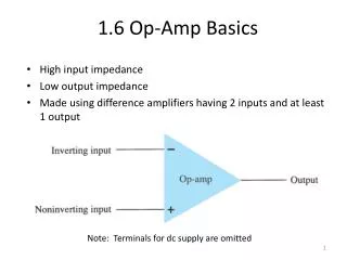
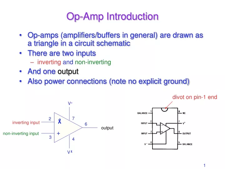
. +. Op-Amp Introduction. Op-amps (amplifiers/buffers in general) are drawn as a triangle in a circuit schematic There are two inputs inverting and non-inverting And one output Also power connections (note no explicit ground). divot on pin-1 end. V +. 7. 2. inverting input. 6.

E N D
+ Op-Amp Introduction • Op-amps (amplifiers/buffers in general) are drawn as a triangle in a circuit schematic • There are two inputs • inverting and non-inverting • And one output • Also power connections (note no explicit ground) divot on pin-1 end V+ 7 2 inverting input 6 output non-inverting input 3 4 V
The ideal op-amp • Infinite voltage gain • a voltage difference at the two inputs is magnified infinitely • in truth, something like 200,000 • means difference between + terminal and terminal is amplified by 200,000! • Infinite input impedance • no current flows into inputs • in truth, about 1012 for FET input op-amps • Zero output impedance • rock-solid independent of load • roughly true up to current maximum (usually 5–25 mA) • Infinitely fast (infinite bandwidth) • in truth, limited to few MHz range • slew rate limited to 0.5–20 V/s
+ Op-amp without feedback • The internal op-amp formula is: Vout = gain(V+ V) • So if V+ is greater than V, the output goes positive • If V is greater than V+, the output goes negative • A gain of 200,000 makes this device (as illustrated here) practically useless V Vout V+
+ Infinite Gain in negative feedback • Infinite gain would be useless except in the self-regulated negative feedback regime • negative feedback seems bad, and positive good—but in electronics positive feedback means runaway or oscillation, and negative feedback leads to stability • Imagine hooking the output to the inverting terminal: • If the output is less than Vin, it shoots positive • If the output is greater than Vin, it shoots negative • result is that output quickly forces itself to be exactly Vin negative feedback loop Vin
+ Positive feedback pathology • In the configuration below, if the + input is even a smidge higher than Vin, the output goes way positive • This makes the + terminal even more positive than Vin, making the situation worse • This system will immediately “rail” at the supply voltage • could rail either direction, depending on initial offset Vin positive feedback: BAD
Op-Amp “Golden Rules” • When an op-amp is configured in any negative-feedback arrangement, it will obey the following two rules: • The inputs to the op-amp draw or source no current (true whether negative feedback or not) • The op-amp output will do whatever it can (within its limitations) to make the voltage difference between the two inputs zero
+ Inverting amplifier example R2 • Applying the rules: terminal at “virtual ground” • so current through R1 is If = Vin/R1 • Current does not flow into op-amp (one of our rules) • so the current through R1 must go through R2 • voltage drop across R2 is then IfR2 = Vin(R2/R1) • So Vout= 0 Vin(R2/R1) = Vin(R2/R1) • Thus we amplify Vin by factor R2/R1 • negative sign earns title “inverting” amplifier • Current is drawn into op-amp output terminal R1 Vin Vout
+ Non-inverting Amplifier R2 • Now neg. terminal held at Vin • so current through R1 is If = Vin/R1 (to left, into ground) • This current cannot come from op-amp input • so comes through R2 (delivered from op-amp output) • voltage drop across R2 is IfR2 = Vin(R2/R1) • so that output is higher than neg. input terminal byVin(R2/R1) • Vout= Vin +Vin(R2/R1) = Vin(1 + R2/R1) • thus gain is (1 + R2/R1), and is positive • Current is sourced from op-amp output in this example R1 Vout Vin
+ Summing Amplifier Rf R1 • Much like the inverting amplifier, but with two input voltages • inverting input still held at virtual ground • I1 and I2 are added together to run through Rf • so we get the (inverted) sum: Vout = Rf(V1/R1 + V2/R2) • if R2 = R1, we get a sum proportional to (V1 + V2) • Can have any number of summing inputs • we’ll make our D/A converter this way V1 R2 Vout V2
+ Differencing Amplifier R2 • The non-inverting input is a simple voltage divider: • Vnode = V+R2/(R1 + R2) • So If = (V Vnode)/R1 • Vout = Vnode IfR2 = V+(1 + R2/R1)(R2/(R1 + R2)) V(R2/R1) • so Vout = (R2/R1)(V V) • therefore we difference V and V R1 V Vout V+ R1 R2
+ Differentiator (high-pass) R • For a capacitor, Q = CV, so Icap = dQ/dt = C·dV/dt • ThusVout = IcapR= RC·dV/dt • So we have a differentiator, or high-pass filter • if signal is V0sint, Vout = V0RCcost • the -dependence means higher frequencies amplified more C Vin Vout
+ Low-pass filter (integrator) C • If = Vin/R, so C·dVcap/dt = Vin/R • and since left side of capacitor is at virtual ground: dVout/dt = Vin/RC • so • and therefore we have an integrator (low pass) R Vin Vout