Download
1 / 23
250 likes | 533 Views
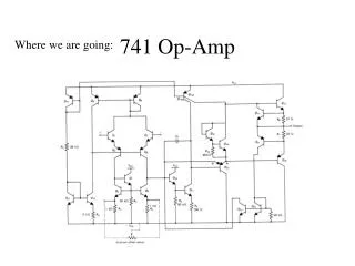
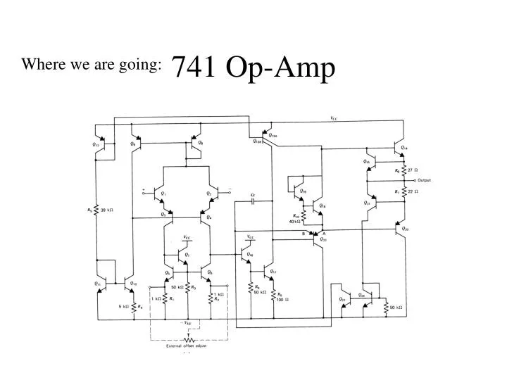
741 Op-Amp. Where we are going:. Why do this?. V out. Higher Linearity Possible Stability. V in. Circuit Element. Why not do this? g m. GND. GND. Lower Bandwidth Higher Noise / D f. Source Degeneration. V out. V in. GND. GND. Source Degeneration. V out.

E N D
741 Op-Amp Where we are going:
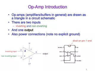
Why do this? Vout • Higher Linearity • Possible Stability Vin Circuit Element Why not do this? gm GND GND • Lower Bandwidth • Higher Noise / Df Source Degeneration Vout Vin
GND GND Source Degeneration Vout Neglect VA of Q1 and assume matched devices: Vout I Vin I = Ieo e V1 /UT = Ieo e(Vin - V1 + Vout/Av )/UT Vin V1 2 V1 = Vin + Vout / Av Q1 I = Ieo e(Vin + Vout/Av )/(2 UT) A similar result for MOSFETs
Vdd GND Common Emitter Common Emitter / Common Source Amplifies the input signal at the output Ibias Assuming an ideal current source: 100mA Vout Ibias = Ico eVin/UT eVout /VA Vin Vout = -VA ln(Ibias/Ico) + - (k VA / UT) Vin
Common Drain Vdd Amplifies the input signal at the output 100pA Ibias Ibias = Ibias ekDVin/UT eDVout/VA Vout Vin DVout = - (k VA / UT) DVin GND Input conductance = 0
Vout Common Drain We must account for the other current source: Vdd Ibias Id = Ibias e-DVout/VAp = Ibias ekDVin/UT eDVout/VAn Vb M6 Vin M7 DVout = - (k (VAn // VAp) UT) DVin GND
Vout Common-Drain: Amplifier Measurements Vdd V1 M6 Ibias Mb M7 GND GND
Common Drain What about above-threshold operation: Vdd Operating region decreases (Vout > Vin - VT) Derive using quadratic functions: 100mA Ibias Vout Ibias = (K/2) ( Vin - VT )2 (1 + (Vout/VA) ) Vin Vout = VA( - 1) GND Amplifies the input signal at the output
High-Gain Amplifier Experiments Load-line Analysis
Vdd Common Base Common Base / Common Gate Amplifies the input signal at the output (non-inverting gain) Ibias Assuming an ideal current source: 100mA Vout Ibias = Ico e (Vb-Vin)/UT eVout /VA Vb Vout = -VA ln(Ibias/Ico) + (VA / UT) Vin - (VA / UT) Vb Vin Gain = VA / UT = Av
Common Gate Vdd Using a subthreshold MOSFET : 100pA Ibias = Io e (kVb-Vin)/UT eVout /VA Ibias Vout = -VA ln(Ibias/Io) + (VA / UT) Vin - (k VA / UT) Vb Vout Vb Gain = VA / UT = Av Vin Problem: Large input current
Vdrain Input resistance of common-gate is low Source is nearly fixed if connected to the drain of a transistor Vin V1 Vgate GND Cascode Circuits Use a common-gate/base transistor to: 1. Improve the output resistance of another transistor. 2. Reduce the Gate-to-Drain capacitance effect of another transistor.
Cascode Circuits Vdrain Vdrain Vbias Vgate GND V1 Vgate Idrain = Io e kVgate/UT e kVbias /VA eVdrain / (Av VA ) GND Idrain = Io e (kVbias-V1)/UT eVdrain /VA = Io e kVgate/UT eV1 /VA V1 ~ kVbias - kVgate + (UT/VA) Vdrain Drain is fixed Fixes the voltage at V1 or isolates V1 from the output
Vdd Cascode Common-Drain Amp One Pole V1 High Output Resistance / DC Gain biasp Vout Ibias biasn Vb Mb GND GND
BJT - CMOS Cascode Circuits Preserve High-gm/I
BJT-MOS Cascades A good way to get zero base current….