Download
1 / 44
450 likes | 536 Views
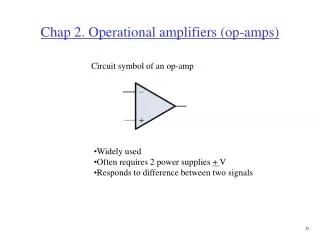
Introduction to Op Amps. ENGI 242 ELEC 222. Basic Op-Amp. The op-amp is a differential amplifier with a very high open loop gain 25k ≤ A VOL ≤ 500k (much higher for FET inputs) high input impedance 500k ≤ Z IN ≤ 10M low output impedance 25 ≤ R O ≤ 100 .

E N D
Introduction to Op Amps ENGI 242 ELEC 222
Basic Op-Amp The op-amp is a differential amplifier with a very high open loop gain 25k ≤ AVOL ≤ 500k(much higher for FET inputs) high input impedance 500k ≤ ZIN≤ 10M low output impedance 25≤RO≤100 ENGI 242/ELEC 222 Op Amps
Op-Amp Equivalent Circuit ENGI 242/ELEC 222 Op Amps
Op-Amp Specifications – DC Offset Parameters • Even though the input voltage is 0, there will be an output. This is called offset. The following can cause this offset: • Input Offset Voltage • Output Offset Voltage due to Input Offset Current • Total Offset Voltage Due to Input Offset Voltage and Input Offset Current • Input Bias Current • See lm301.pdf or mc1741c.pdf for sample specification sheets ENGI 242/ELEC 222 Op Amps
General Op-Amp Specifications VIO • Input Offset Voltage VIO • The voltage that must be applied to the input terminals of an op amp to null the output voltage • Typical value is 2mV with a max of 6mV • When operated open loop, must be nulled or device may saturate ENGI 242/ELEC 222 Op Amps
General Op-Amp Specifications IIO • Input Offset Current • The algebraic difference between the two input currents • These are base currents and are usually nulled • Typical value IIO 20 nA with a max of 200nA ENGI 242/ELEC 222 Op Amps
Technique to Null VO • Short Input terminals to ground • Connect potentiometer between compensation pins with wiper to VEE • Potentiometer is usually a 10 turn device • Connect meter to output and adjust potentiometer for VO = 0 ENGI 242/ELEC 222 Op Amps
General Op-Amp Specifications CMRR • Common Mode Rejection Ratio • The ratio of the differential voltage gain (AD) to the common mode gain (ACM) • ACM is the ratio between the differential input voltage (VINCM) applied common mode, and the common mode output voltage (VOCM) • it can exceed minimum is 70db with a typical value of 90 db • in properly designed circuit, it may exceed 110db ENGI 242/ELEC 222 Op Amps
General Op-Amp Specifications • Input Bias Current • The average of the currents that flow into the inverting and noninverting terminals • Typical values rage from 7nA to 80 nA • Differential Input Resistance • Also know as the input resistance • Resistance seen looking into the input terminals of the device • Runs from a low of 2M for an LM741 to a high of 1012 for FET input devices • Output resistance • Resistance between the output terminal ad ground • Typical values are 75 or less • Input Capacitance • The equivalent capacitance measured at either the inverting or noninverting terminal with the other terminal connected to ground • May not be on all spec sheets • Typical value for LM741 is 1.4pF ENGI 242/ELEC 222 Op Amps
General Op-Amp Specifications • Power Supply Range • May be differential or single ended • Max is ± 22V • Output Voltage Swing • Range of output voltage • Depends on power supply voltage used (typically about 85% to 90%) • Usually about ±13.5V for a power supply voltage of ±15V • Slew Rate • The maximum rate of change in the output voltage in response to an input change • Depends greatly on device, higher is better (output resonds faster to input changes) • For LM741 it is .5V/s while for the LM318 it is 70V /s • Gain Bandwidth Product • The bandwidth of the device when the open loop voltage gain is 1 ENGI 242/ELEC 222 Op Amps
Op Amp Equivalent Circuit ENGI 242/ELEC 222 Op Amps
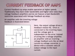
Op-Amp Gain • Op-Amps have a very high gain. They can be connected open- or closed loop. • Open-loop (AVOL) refers to a configuration where there is no feedback from output back to the input • AVOL may exceed 10,000 • Closed-loop (AVCL) configuration reduces the gain In order to control the gain of an op-amp it must have negative feedback • Negative feedback will reduce the gain and improve many characteristics of the op-amp ENGI 242/ELEC 222 Op Amps
Typical Op Amp Frequency Response ENGI 242/ELEC 222 Op Amps
Change in AV with Feedback ENGI 242/ELEC 222 Op Amps
Virtual Ground Since ZIN is very high, we assume no current can flow into any lead of the op amp When the non-inverting input pin is at ground, the inverting input pin is at 0V The equivalent circuit. ENGI 242/ELEC 222 Op Amps
Practical Op-Amp Circuits • Typical Op-amp circuit configurations include the: • Unity Gain Buffer (Voltage Follower) • Inverting Amplifier • Noninverting Amplifier • Summing Amplifier • Integrator • Differentiator • Note: the integrator and differentiator are considered active filters ENGI 242/ELEC 222 Op Amps
Unity Gain Buffer (Follower) ENGI 242/ELEC 222 Op Amps
Inverting Op Amp The input is applied to the inverting (-) input the non-inverting input (+) is grounded RF is the feedback resistor, and is connected from the output to the inverting input This is called negative feedback ENGI 242/ELEC 222 Op Amps
Inverting Op Amp We assume that no current enters the inverting terminal II- < 100nA VD 0V ENGI 242/ELEC 222 Op Amps
Inverting Op-AmpGain Closed Loop Gain is controlled by the external resistors: RF and R1 For Unity Gain: AV is -1 and RF = R1 The minus sign denotes a 180 degree phase shift between input and output ENGI 242/ELEC 222 Op Amps
Inverting Op Amp Compensated for Ibias R is used to compensate for difference in IBIAS+ and IBIAS- ENGI 242/ELEC 222 Op Amps
Inverting Op-Amp A This configuration achieves high gain with a smaller range of resistor values than the basic inverter V- V+ ENGI 242/ELEC 222 Op Amps
Inverting Amplifier with High Zin Use a Unity Gain Buffer to obtain a very high input resistance with an inverting amplifier ENGI 242/ELEC 222 Op Amps
Inverting Amplifier for Low RL Use a Unity Gain Buffer to obtain a very high input resistance to drive a low impedance load ENGI 242/ELEC 222 Op Amps
Noninverting Amplifier V- = V+ = vi ENGI 242/ELEC 222 Op Amps
Noninverting Op Amp Compensated for IBIAS Rbias is used to compensate for difference in IBIAS+ and IBIAS- ENGI 242/ELEC 222 Op Amps
Differential (Difference) Amplifier A V1 V2 A ENGI 242/ELEC 222 Op Amps
Differential Amplifier Output ENGI 242/ELEC 222 Op Amps
Instrumentation Amplifier Buffered Input R1 = R2, RF1 = RF2 ENGI 242/ELEC 222 Op Amps
Instrumentation Amplifier R1 = R2, RF1 = RF2 ENGI 242/ELEC 222 Op Amps
Inverting Summing Amplifier • By applying KCL to the multiple inputs, we can consider the contribution of each source individually • IF + I- = I1 + I2 + I3 • but I- 0 • IF = I1 + I2 + I3 VO = -IF RF ENGI 242/ELEC 222 Op Amps
Non-inverting Summing Amplifier Perform a source transformation for each input Sum the current sources and find RTH for the resistances VIN+ = IT RTH ENGI 242/ELEC 222 Op Amps
Integrator The output is the integral of the input This circuit is a low-pass filter circuit, and is used and sensor conditioning circuits ENGI 242/ELEC 222 Op Amps
Differentiator The differentiator takes the derivative of the input This circuit is a high-pass filter circuits ENGI 242/ELEC 222 Op Amps
Comparator • High Gain Op Amp • Operated Open Loop • Designed to compare an input to a reference voltage • Gives output (digital level) to indicate if input is above or below reference • Circuit designed to give VOSAT and –VOSAT only ENGI 242/ELEC 222 Op Amps
Comparator Operation Example ENGI 242/ELEC 222 Op Amps
LM 311 Comparator ENGI 242/ELEC 222 Op Amps
Window Comparator ENGI 242/ELEC 222 Op Amps
Determine the Output ENGI 242/ELEC 222 Op Amps
Block Diagram of 555 ENGI 242/ELEC 222 Op Amps
Astable Multivibrator ENGI 242/ELEC 222 Op Amps
555 Used as an Astable Multivibrator ENGI 242/ELEC 222 Op Amps
Schmidt Trigger 7414 • A Schmidt trigger (a comparator with Hysteresis) is a bistable digital (two-state) device • It accepts virtually any analog input and provides a logic 0 or 1 output • A typical use is to take distorted digital signals (due to RC time constant of transmission line) and provide a used to square-wave output • Can be used to eliminate noise near reference point that would cause problems in analog comparators ENGI 242/ELEC 222 Op Amps
Hysteresis ENGI 242/ELEC 222 Op Amps