Download
1 / 22
230 likes | 581 Views
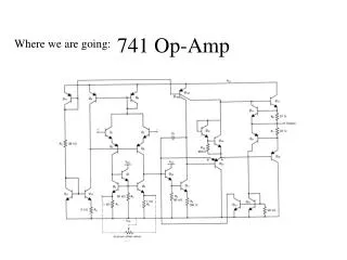
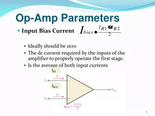
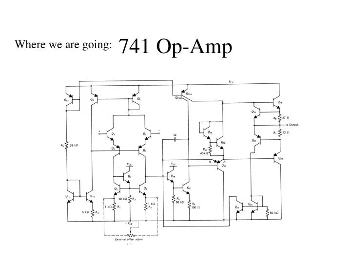
741 Op-Amp. Where we are going:. Typical CMOS Amplifier. Drain Characteristics. I out. Current Sink. V out. V b. M 5. GND. V dd. Current Source. V 1. M 6. I out. Current Sources. Ever wonder how we make one of these?. How “good” a current source?. GND.

E N D
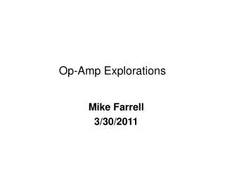
741 Op-Amp Where we are going:
Iout Current Sink Vout Vb M5 GND Vdd Current Source V1 M6 Iout Current Sources Ever wonder how we make one of these? How “good” a current source?
GND Current versus Drain Voltage Not flat due to Early effect (channel length modulation) Id = Id(sat) (1 + (Vd/VA) ) Ic = Ic(sat) (1 + (Vc/VA) ) Iout or Id = Id(sat) eVd/VA Rout 10mA Ic = Ic(sat) eVc/VA
Iout Iin Vdd Vdd Vout Vb Vb M4 M7 Mb M5 Iout GND GND Iin Current Mirrors nFET Current Mirror pFET Current Mirror Iout = ( (W/L)5 / (W/L)b) Iin Iout = ( (W/L)7 / (W/L)4) Iin A good way to generate a bias current
Current Mirror Iout1 Iout2 Iout3 Iin Vout1 Vout2 Vout3 Vb Mb M5 M6 M7 GND GND GND GND Iout / Iin = ( (W/L)7 / (W/L)b) Iout / Iin = ( (W/L)6 / (W/L)b) Iout = ( (W/L)5 / (W/L)b) Iin
Basic One-Transistor Circuits Common Source Common Gate Source Follower Common Emitter Common Base Emitter Follower The fundamental two-transisor circuit: Differential Pair
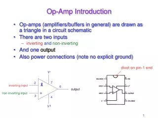
Signal Flow in Transistors • Rules of Thumb • The collector or drain can never be an input terminal. • The base or gate can never be an output terminal. • In addition it is important to note polarity reversals on these signal paths. • The base-collector or gate-drain path inverts. • All other paths are noninverting. • (This of course assumes that there are no reactive elements causing phase shifts) (Never is too strong a word)
Vdd Vdd Vdd GND GND GND Spectrum of Amplifier “Loads” 10mA R1 Vb Vout Vout Vout Vin Vin Vin Ideal Current Source Load Transistor Current Source Load Resistive Load Remember: On-chip resistors are expensive
Vdd Vdd GND Multiple Transistor Configurations Vdd 100pA 500mA 10mA Vout Vout Vout Vin Vin Vin GND GND Subthreshold MOS Above threshold MOS BJT JFETs as well….
Vdd GND Source or Emitter Follower Ideal current source BJT or Subthreshold MOSFET: Vin Iref = Ieo e(Vin -Vout )/UT Vout = -UT ln(Ibias/Ieo) + Vin Vout or 100mA Iref = Iref e(DVin -DVout )/UT D Vout = D Vin (SubVT MOS: D Vout = kD Vin ) Vdd MOS (Above VT MOS ): Vin Vout Iref = (K/2) ( Vin - Vout - VT )2 10nA Vout = Vin – sqrt(2 Iref / K) ) GND
GND GND Small-Signal Analysis (CD or CC) + V - Vin Vout rp (Vin - Vout ) / rp + (Vin - Vout ) gm = Vout / ro ro gmV BJT (ro >> rp) MOS (rp = 0) Vout/Vin = 1/(1 + [(rp / ro)/(1 + rp gm)]) Vout (1 + ro gm) ~ ro gmVin Vout/Vin ~ 1/(1 + [(rp / ro)/(rp gm)]) = 1/(1 + 1 / (rp gm) ) = 1/(1 + UT / VA ) ~ 1 Vout/Vin = 1/(1 + 1 / (rp gm) ) = 1/(1 + UT / VA ) ~ 1
Vdd GND Common Drain or Emitter Ideal current source BJT or Subthreshold MOSFET: Iref 100mA Ibias = Ico eVin/UT eVout /VA Vout Vin Vout = -VA ln(Ibias/Ico) + - (k VA / UT) Vin Ibias = Ibias ekDVin/UT eDVout/VA Vdd DVout = - (k VA / UT) DVin 100pA MOS (Above VT MOS ): Iref Operating region decreases (Vout > Vin - VT) Derive using quadratic functions: Vout Vin GND Ibias = (K/2) ( Vin - VT )2 (1 + (Vout/VA) )
Common Drain Vdd Amplifies the input signal at the output 100pA Ibias Ibias = Ibias ekDVin/UT eDVout/VA Vout Vin DVout = - (k VA / UT) DVin GND Input conductance = 0
Vout Common Drain We must account for the other current source: Vdd Ibias Id = Ibias e-DVout/VAp = Ibias ekDVin/UT eDVout/VAn Vb M6 Vin M7 DVout = - (k (VAn // VAp) UT) DVin GND
Common Drain What about above-threshold operation: Vdd Operating region decreases (Vout > Vin - VT) Derive using quadratic functions: 100mA Ibias Vout Ibias = (K/2) ( Vin - VT )2 (1 + (Vout/VA) ) Vin GND
Vdd Common Base Common Base / Common Gate Amplifies the input signal at the output (non-inverting gain) Ibias Assuming an ideal current source: 100mA Vout Ibias = Ico e (Vb-Vin)/UT eVout /VA Vb Vout = -VA ln(Ibias/Ico) + (VA / UT) Vin - (VA / UT) Vb Vin Gain = VA / UT = Av
Common Gate Vdd Using a subthreshold MOSFET : 100pA Ibias = Io e (kVb-Vin)/UT eVout /VA Ibias Vout = -VA ln(Ibias/Io) + (VA / UT) Vin - (k VA / UT) Vb Vout Vb Gain = VA / UT = Av Vin Problem: Large input current
Vdrain Input resistance of common-gate is low Source is nearly fixed if connected to the drain of a transistor Vb V1 Vgate GND Cascode Circuits Use a common-gate/base transistor to: 1. Improve the output resistance of another transistor. 2. Reduce the Gate-to-Drain capacitance effect of another transistor.
Cascode Circuits Vdrain Vdrain Vbias Vgate GND V1 Vgate Idrain = Io e kVgate/UT e kVbias /VA eVdrain / (Av VA ) GND Idrain = Io e (kVbias-V1)/UT eVdrain /VA = Io e kVgate/UT eV1 /VA V1 ~ kVbias - kVgate + (UT/VA) Vdrain Drain is fixed Fixes the voltage at V1 or isolates V1 from the output
Vdd Cascode Common-Drain Amp One Pole V1 High Output Resistance / DC Gain biasp Vout Ibias biasn Vb Mb GND GND