Download
1 / 31
340 likes | 405 Views
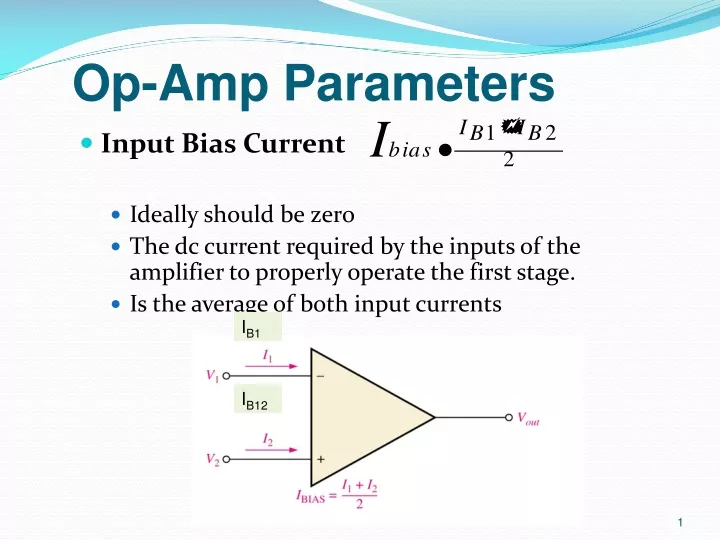
Op-Amp Parameters. Input Bias Current Ideally should be zero The dc current required by the inputs of the amplifier to properly operate the first stage. Is the average of both input currents. I B1. I B12. Op-Amp Parameters. Input Bias Current Range 10 to 100 nA for BJT

E N D
Op-Amp Parameters • Input Bias Current • Ideally should be zero • The dc current required by the inputs of the amplifier to properly operate the first stage. • Is the average of both input currents IB1 IB12
Op-Amp Parameters • Input Bias Current • Range 10 to 100 nA for BJT • Range 1 to 10 pA for JFET • Reason : It is undesirable voltage drop in the resistors forming feedback network
Op-Amp Parameters • Input Offset Current (IOS) • Is the difference of input bias currents IB1 IB12 • Reason : It is due to lack of perfect symmetry in input differential stage
Op-Amp Parameters • Input Offset Current (IOS) • Range 20 to 60 nA for BJT
Op-Amp Parameters • Input Offset Voltage [Vos] • Ideally, output of an op-amp is 0 Volt if the input is 0 Volt. • Realistically, a small dc voltage will appear at the output when no input voltage is applied. • Thus, differential dc voltage is required between the inputs to force the output to zero volts. • This is called the Input Offset Voltage, Vos.
Op-Amp Parameters • Input Offset Voltage [Vos] • It is input voltage which must be applied across the input terminals to obtain zero output voltage. • It can be nulled by a external potentiometer.
Op-Amp Parameters • Input Offset Voltage [Vos] • Range between 2 mV to 5 mV.
Op-Amp Parameters • Input Offset Current • Is the difference of input bias currents Input offset current Offset voltage Thus, error
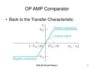
Op-Amp Parameters • Common-Mode Rejection Ratio (CMRR) • The ability of amplifier to reject the common-mode signals (unwanted signals) while amplifying the differential signal (desired signal) • Ratio of open-loop gain, Adm to common-mode gain, Acm • The open-loop gain is a datasheet value • The higher the CMRR, the better, in which the open-loop gain is high and common-mode gain is low.
Op-Amp Parameters • Common-Mode Rejection Ratio (CMRR) • CMRR is usually expressed in dB • Range 60 to 100 dB
Op-Amp Parameters • Common-Mode Input Voltage • It is the maximum range of input voltage that can be simultaneously applied to both inputs without causing cut off or saturation of amplifier stages. • The range of input voltages which, when applied to both inputs, will not cause clipping or other output distortion.
Op-Amp Parameters • Difference -Mode Input Voltage • It is the maximum range of differential signal voltage that can be safely applied to the OpAmp input signal.
Supply Voltage Rejection Ratio (SVRR) One of the reasons OpAmps are so useful, is that they can be operated from a wide variety of power supply voltages. The 741 op amp can be operated from bipolar supplies ranging from 5V to 18V without too many changes to the parameters of the op amp.
Supply Voltage Rejection Ratio The supply voltage rejection ratio (SVRR) refers to the slight change in input offset voltage per volt change in power supply of the opamp. SVRR = VOS / VCC) Range 10-5 to7 10-5
Op-Amp Parameters • Input Impedance • Is the total resistance between the inverting and non-inverting inputs. • Differential input impedance : total resistance between the inverting and non-inverting inputs • Common-mode input impedance: total resistance between each input and ground Range 100 k to 1 M
Op-Amp Parameters • Output Impedance • Ideally should be zero • Is the resistance viewed from the output terminal of the op-amp. In reality, it is non-zero. Range 40 k to 100
Op-Amp Parameters • Slew Rate • Is the maximum rate of change of the output voltage in response to a step input voltage.
Op-Amp Parameters • Slew Rate • It’s a measure of how fast the output can “follow” the input signal. Range 50 mV/Sec to 500 mV/Sec
Op-Amp Parameters • Example Determine the slew rate:
Output Voltage Swing Max p-p output which can be obtain without waveform clipping Range 50 to 80 % of supply voltage It depends on supply voltage This parameters is useful in switching application.
Unity Gain bandwidth In practice, the voltage gain decrease at high frequency. The frequency at which the open loop voltage gain becomes equal to Unity Gain bandwidth. Range 1 to 20 MHz
Unity Gain bandwidth Frequency at which the open loop voltage gain becomes equal to unity Range 1 to 20 MHz
Full power bandwidth The maximum frequency over which the full output voltage swing can be obtained.
Overload Recovery time It is time required for the output stage to return to active region when drives to active hard saturation. It depends upon the degree of overload and feedback impedance.
VE = VIN+ - VIN- VOUT = a * VE VIN- VIN+
Input Common Mode Voltage Range VICR - Average voltage at the inverting and noninverting input pins
Differential Input Voltage Range Absolute Maximum Rating