Download
1 / 22
250 likes | 464 Views
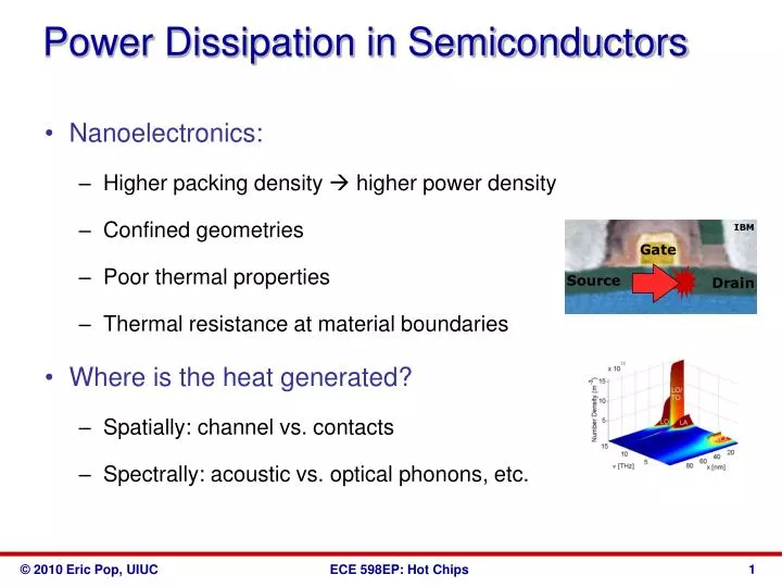
Power Dissipation in Semiconductors. Nanoelectronics: Higher packing density higher power density Confined geometries P oor thermal properties Thermal resistance at material boundaries Where is the heat generated ? Spatially: channel vs. contacts

E N D
Power Dissipation in Semiconductors • Nanoelectronics: • Higher packing density higher power density • Confined geometries • Poor thermal properties • Thermal resistance at material boundaries • Where is the heat generated? • Spatially: channel vs. contacts • Spectrally: acoustic vs. optical phonons, etc.
Simplest Power Dissipation Models R • Resistor: P = IV = V2/R = I2R • Digital inverter: P = fCV2 • Why?
Revisit Simple Landauer Resistor Ballistic Diffusive ? I = q/t P = qV/t = IV µ1 µ1 E E µ2 µ2 µ1-µ2 = qV Q: Where is the power dissipated and how much?
Continuum View of Heat Generation • Lumped model: • Finite-element model: • More complete finite-element model: µ1 (phonon emission) E (recombination) µ2 be careful: radiative vs. phonon-assisted recombination/generation?!
Most Complete Heat Generation Model Lindefelt (1994): “the final formula for heat generation” Lindefelt, J. Appl. Phys. 75, 942 (1994)
Computing Heat Generation in Devices • Drift-diffusion: • Does not capture non-local transport • Hydrodynamic: • Needs some avg. scattering time • (Both) no info about generated phonons H (W/cm3) y (mm) x (mm) • Monte Carlo: • Pros: Great for non-equilibrium transport • Complete info about generated phonons: • Cons: slow(there are some short-cuts)
Details of Joule Heating in Silicon E > 50 meV t~ 0.1ps 60 E < 50 meV optical (vop≤ 1000 m/s) t~ 0.1ps 50 Optical Phonons 40 t ~ 10 ps 30 Acoustic Phonons (vac ~ 5-9000 m/s) 20 t~ 1 ms – 1 s 10 acoustic Heat Conduction to Package IBM High Electric Gate Field Source Drain Hot Electrons (Energy E) Freq (Hz) Energy (meV) Wave vector qa/2p
Self-Heating with the Monte Carlo Method • Electrons treated as semi-classical particles, not as “fluid” • Drift (free flight), scatter and select new state • Must run long enough to gather useful statistics • Main ingredients: • Electron energy band model • Phonon dispersion model • Device simulation: • Impurity scattering, Poisson equation, boundary conditions • Must set up proper simulation grid
Monte Carlo Implementation: MONET E. Pop et al., J. Appl. Phys. 96, 4998 (2004) optical • Analytic electron energy bands + analytic phonon dispersion • First analytic-band code to distinguish between all phonon modes • Easy to extend to other materials, strain, confinement 50 meV Typical MC codes Our analytic approach Analytic band Phonon Freq. w (rad/s) Density of States (cm-3eV-1) Full band 20 meV OK to use acoustic Wave vector qa/2p Energy E (eV)
g f 1.5 (LA, 19 meV) 7.0 (LO, 64 meV) Pop, 2004 3.0 (LA/LO, 51 meV) 1.5 (TO, 57 meV) Inter-Valley Phonon Scattering in Si • Six phonons contribute • well-known: phonon energies • disputed: deformation potentials • What is their relative contribution? • Rate: • Include quadratic dispersion for all intervalley phonons w(q)= vsq-cq2 Deformation Potentials Dp (108 eV/cm) 0.5 (TA, 10 meV) 0.8 (LA, 18 meV) 11.0 (LO, 63 meV) g-type 0.3 (TA, 19 meV) 2.0 (LA/LO, 50 meV) 2.0 (TO, 59 meV) f-type Jacoboni, 1983
SKIP Herring & Vogt, 1956 Intra-Valley Acoustic Scattering in Si (XTA/vTA)2 • q= angle between phonon k and longitudinal axis • Averaged values: DLA=6.4 eV, DTA=3.1 eV, vLA=9000 m/s, vTA=5300 m/s (XLA/vLA)2 longitudinal Yoder, 1993 Fischetti & Laux, 1996 Pop, 2004
SKIP Scattering and Deformation Potentials E. Pop et al., J. Appl. Phys. 96, 4998 (2004) Inter-valley Intra-valley Herring & Vogt, 1956 Yoder, 1993 Fischetti & Laux, 1996 This work (isotropic, average over q) Average values: DLA = 6.4 eV, DTA = 3.1 eV (Empirical Xu = 6.8 eV, Xd = 1eV) * old model = Jacoboni 1983 **consistent with recent ab initio calculations (Kunikiyo, Hamaguchi et al.)
Mobility in Strained Si on Si1-xGex 2 Strained Si Bulk Si 4 Strained Si on Relaxed Si1-xGex 6 Es ~ 0.67x biaxial tension 4 2 Conduction Band splitting + repopulation Less intervalley scattering Smaller in-plane mt<ml Largerμ=qt/m* !!! Various Data (1992-2002) Simulation
Computed Phonon Generation Spectrum E. Pop et al., Appl. Phys. Lett. 86, 082101 (2005) • Complete spectral information on phonon generation rates • Note: effect of scattering selection rules (less f-scat in strained Si) • Note: same heat generation at high-field in Si and strained Si
Strained Si x=0.3, DE=0.2 eV Doped 1017 Bulk Si Phonon Generation in Bulk and Strained Si E. Pop et al., Appl. Phys. Lett. 86, 082101 (2005) bulk Si • Longitudinal optical (LO) phonon emission dominates, but more so in strained silicon at low fields (90%) • Bulk silicon heat generation is about 1/3 acoustic, 2/3 optical phonons strained Si
1-D Simulation: n+/n/n+ Device (including Poisson equation and impurity scattering) N+ N+ i-Si V qV
Heat Gen. (eV/cm3/s) MONET MONET DL Medici Medici Error: DL/L = 0.10 DL/L = 0.38 DL/L = 0.80 1-D Simulation Results Potential (V) L=500 nm 100 nm 20 nm MONET Medici • MONET vs. Medici (drift-diffusion commercial code): • “Long” (500 nm) device: same current, potential, nearly identical • Importance of non-local transport in short devices (J.Emethod insufficient) • MONET:heat dissipation in DRAIN (optical, acoustic) of 20 nm device
Heat Generation Near Barriers Lake & Datta, PRB 46 4757 (1992) Heating near a single barrier Heating near a double-barrier resonant tunneling structure
Heat Generation in Schottky-Nanotubes Ouyang & Guo, APL 89 183122 (2006) • Semiconducting nanotubes are Schottky-FETs • Heat generation profile is strongly influenced by barriers • +Quasi-ballistic transport means less dissipation
Are Hot Phonons a Possibility?! L = 20 nm • Hot phonons: if occupation (N) >> thermal occupation • Why it matters: added impact on mobility, leakage, reliability • Longitudinal optical (LO) phonon “hot” for H > 1012 W/cm3 • Such power density can occur in drain of L ≤ 20 nm, V > 0.6 V device V = 0.2, 0.4, 0.6, 0.8, 1.0 V source drain where and
Last Note on Phonon Scattering Rates • Note, the deformation potential (coupling strength) is the same between phonon emission and absorption • The differences are in the phonon occupation term and the density of final states • What if kBT >> ħω (~acoustic phonons)? • What if kBT << ħω (~optical phonons)? • Sketch scattering rate vs. electron energy:
Sketch of Scattering Rates vs. Energy emission Γ=1/τ Γ=1/τ emission ≈ absorption absorption E ħω E kBT » ħω Nq « 1 Γ ~ g(E) ~ E1/2 in 3-D, etc. kBT « ħω Nq » 1 Γ ~ Nqg(E± ħω) ~ (E ± ħω)1/2 in 3-D Note emission threshold E > ħω