Download
1 / 19
210 likes | 328 Views
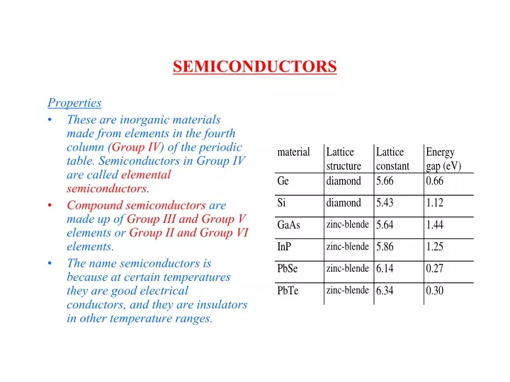
SEMICONDUCTORS. Properties These are inorganic materials made from elements in the fourth column ( Group IV ) of the periodic table. Semiconductors in Group IV are called elemental semiconductors .

E N D
SEMICONDUCTORS Properties • These are inorganic materials made from elements in the fourth column (Group IV) of the periodic table. Semiconductors in Group IV are called elemental semiconductors. • Compound semiconductors are made up of Group III and Group V elements or Group II and Group VI elements. • The name semiconductors is because at certain temperatures they are good electrical conductors, and they are insulators in other temperature ranges.
The most important semiconductor is Si because of its wide use in IC and MEMS fabrication. - Si crystallizes in diamond lattice. - Each Si atom has four equi-distant nearest neighbors. - The lattice constant for Si is 5.43 Å.
Silicon Growth : Starting Materials • A relatively pure form of sand (SiO2) called quartzite is placed in a furnace with various forms of carbon (e .g., coal, coke, and wood chips). The overall reaction is SiC (solid) + SiO2 Si (solid) + SiO (gas) + CO (gas) • Next the Si is treated with HCl to form trichlorosilane (SiHCl3) Si (solid) + 3HCl (gas) SiHCl3 (gas) + H2 (gas) • The trichlorosilane is liquid at room temperature (boiling point 32 °C). Fractional distillation of the liquid removes the unwanted impurities. • The purified trichlorosilane is then used in a hydrogen reduction reaction to prepare electronic-grade silicon (EGS) ; SiHCl3 (gas) + H2 (gas) Si (solid) + 3HCl (gas) • EGS so prepared is polycrsytalline of high purity and is used as the raw material for the preparation of Czochralski single-crystal Si. 300 °C
Silicon Growth from the Melt (Czochralski Technique) • The Czochralski technique for Si growth uses an apparatus called a puller. • In the crystal growing process, poly-Si is placed in the crucible and the furnace is heated above the melting temperature of Si. • A suitably oriented seed crystal [e. g., (100)] is suspended over the crucible in a seed holder. • The seed is inserted into the melt. Part of it melts, but the tip of the remaining seed still touches the liquid surface.The seed is then slowly withdrawn(pulled). A typical pull rate is a few mm/min. • Progressive freezing at the solid-liquid interface yield a large single crystal. • In crystal growth, a known amount of dopant is added to the melt to obtain the desired doping concentration in the grown crystal.
Wafer Identification, Diameter, and Thickness • After the crystal is grown, the next operation is to grind the surface so that the diameter of the material is defined. • Typical wafer diameters are 2, 4, 6 or 8 inches. • After that one or more flat regions are ground along the length of the ingot. These flats mark the specified crystal orientation of the ingot and the conductivity type of the material. • The ingot is then sliced by diamond saw into wafers. Slicing determines surface orientation, thickness, and taper. • Typical wafer thicknesses are 250, 525, or 650 mm. • The wafer is then lapped using a mixture of alumina and glycerine to produce a typical flatness uniformity within 2 mm. • The wafer is then "etched" and polished to produce a smooth, specular surface.
Intrinsic Silicon • Charge carriers in semiconductors are electrons and positively charged holes (magnitude of charge is the same as that in electron). • In an intrinsic semiconductor, the concentrations of electrons (n) and holes (p) are equal to each other : n = p = ni (intrinsic carrier concentration). • Resistivity, r, for an intrinsic semiconductor is given by • r = [nie(mn + mp)]-1,where mn(p) are the electron (hole) mobility. • For Si, at room temperature:ni~ 1010 cm-3 , and mn(p) ~103 cm2/Vs. Hence, r~105 W cm.
N-Type Silicon (Extrinsic Silicon) • In n-type Si electrical conduction is carried out by electrons. • Dopants are atoms from Group V elements, most common dopants are P and As. • The dopant atoms are called donor atoms since they donate their fifth electron to the Si crystal. • The resistivity of an n-type Si material can be several orders of magnitude smaller than the intrinsic resistivity of Si.
P-Type Silicon (Extrinsic Silicon) • In p-type Si electrical conduction is carried out by holes. • Dopants are atoms from Group III elements, most common dopants are B and Al. • The dopant atoms are called acceptor atoms since each atom accepts an electron and gives away a free hole to the Si crystal. • The resistivity of a p-type Si material can be several orders of magnitude smaller than the intrinsic resistivity of Si.
Si Film Growth : Epitaxial Processes • The method used for growing Si layer on a substrate wafer is epitaxial process where the substrate wafer acts as a seed crystal. • Common epitaxial processes are vapor phase epitaxy (VPE) and molecular beam epitaxy (MBE). VPE
In VPE several silicon sources are usually used : silicon tetrachloride (SiCl4), dichlorosilane (SiH2Cl2), trichlorosilane (SiHCl3), and silane (SiH4). • e. g., (SiCl4) • -Typical reaction temperature for SiCl4 is ~ 1200 °C. • - The Si layer formation reaction is • SiCl4 (gas) + 2H2 (gas) Si (solid) + 4HCl • - A competing reaction which occurs simultaneously SiCl4 (gas) + Si (solid) 2SiCl2 (gas) • - Hence if the concentration of SiCl4 is too high, material removal rather than growth of Si takes place.
Crystal Characterization • The grown Si wafer differs from an ideal crystal in many ways : • It is finite so surface atoms are not completely bonded. • It has defects such as : (I) point defects, (ii) line defects, (iii) area defects, and (iv) volume defects.
CERAMIC MATERIALS • These are inorganic materials which consist of metallic and non-metallic elements chemically bonded together. Examples are alumina (Al2O3), salts such as sodium chloride (NaCl) and ceramic superconductors such as YBa2Cu3O6.5 . • Most ceramics, being them single-crystalline or amorphous (glass) have high hardness, and high-temperature strength, but tend to have mechanical brittleness.
POLYMERIC MATERIALS • Polymers are materials that are organic (containing carbon) which have long molecular chains or networks. Examples; epoxies, polysters, nylons, and silicones. • Most polymers are poor conductors of electricity. In fact some polymers are excellent insulators. • Polymers have low densities and relatively low softening or decomposition temperatures. • Since polymers are either long snake-like structures or three-dimensional random networks polymeric materials are usually non-crystalline. However one may still find some single-crystal polymers. • Single crystal properties are encountered also in some polymers, however single crystallinity in these polymers is only partial. The development of single crystallinity in polymers is important because of its effects on mechanical, thermal, and optical properties. • Single crystallinity in polymers is achieved by forming long molecules such as chains of many thousands of carbon atoms by chemical reaction. Upon cooling from liquid these molecules bend back and forth to form individual crystals.
ELECTRONIC MATERIALS • To fabricate ICs and MEMS many different kinds of bulk materials and thin films are used. • The bulk materials are predominantly semiconductors. • The most important semiconductor for ICs and MEMS is Si. • Thin films in ICs and MEMS are classified into four groups : Thin films thermal SiO2 dielectrics Poly-Si metals deposited SiO2 deposited Si3N4
Thermal Oxidation For Silicon Dioxide (SiO2) Film Formation • The setup comprises a resistance heated furnace, a cylindrical fused-quartz tube containing Si wafers held vertically in slotted quartz boat, and a source of either dry oxygen or water vapor. • Several dozen wafers typically stand vertically ~ 1 cm apart and are oxidized simultaneously. • Temperature is controlled to within ± 1 °C.
At the wafer surface Si combines with oxygen to form the oxide Si (solid) + O2 (gas) SiO2 (Solid) Or Si (solid) + 2H2O (gas) SiO2 (solid) + 2H2 (gas) Si is consumed in this process, and subsequently Si surface recedes from its original location. However, the volume of grown oxide is larger than that of consumed Si (consumed Si volume/grown oxide volume ~ 0.44); i. e., the net effect is an increase in thickness. 900 °C to 1200 °C 900 °C to 1200 °C
The basic structural unit of thermal oxide is a Si atom surrounded tetrahedrally by four oxygen atoms. • The Si-O and O-O internuclear distances are 1.6 Å and 2.27 Å, respectively. • SiO2 or silica has several crystalline structures (the dominant one is quartz), and an amorphous structure. • Amorphous oxide has a density of ~ 2.2 gm/cm3, whereas quartz has a density of ~ 2.7 gm/cm3. • Thermally grown oxides are usually amorphous.