Download
1 / 27
340 likes | 750 Views
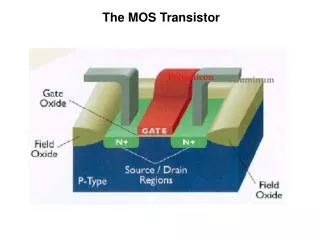
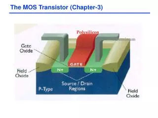
ECE 431 Digital Circuit Design Chapter 3 MOS Transistor (MOSFET). (slides 2: key Notes) Lecture given by Qiliang Li. Introduction. Metal Oxide Semiconductor Field Effect Transistor (MOSFET) is the fundamental building block for modern digital integrated circuit and analog circuit.

E N D
ECE 431 Digital Circuit DesignChapter 3 MOS Transistor (MOSFET) (slides 2: key Notes) Lecture given by Qiliang Li
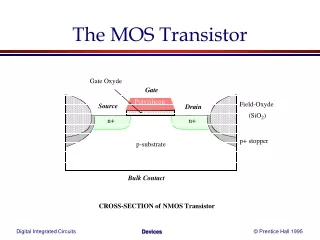
Introduction • Metal Oxide Semiconductor Field Effect Transistor (MOSFET) is the fundamental building block for modern digital integrated circuit and analog circuit. MOS structure I-V Characteristics of MOSFET MOSFET scaling and short-channel effect MOSFET capacitance
Energy band diagrams of the components of MOS structure qVFB Flat-band voltage
Example 1 for MOS structure The electron affinity of silicon is 4.15eV For a p-Si: , gate metal is Al: , what is VFB? An: 4.1eV 4.15eV Ec 0.55eV VFB Ei 0.2eV EFp Ev Al Si
Start of Strong Inversion. MOSFET starts to turn on. Threshold Voltage Body-effect coefficient
Depletion region charge at VSB = 0 for p-Si Negative b/c hole is depleted for n-Si Positive b/c electron is depleted Oxide fixed charge is positive Qox > 0
Example 2 Find VT0 and VT N-channel MOSFET Substrate Na=1E16 cm-3 Poly-Si gate Nd=2E20 cm-3 Tox=50 nm Oxide interface fixed charge density Nox=4E10 cm-3
3.4 MOSFET I-V Characteristics Why it is negative? n channel
Resistance of tiny part of the channel dy : Voltage drop across dy :
Example 3 Saturation? Find the maximum
Channel length modulation effect Channel length modulation effect: The effective channel length during saturation is significantly shorter than before saturation.
Example 4 from Eq 3.23
3.5 MOSFET Scaling and Small-Geometry Effects Full Scaling (Constant-Field Scaling) Capacitance ? Cox W L -> 1/S Time delay tdelay Power = IDD VDD
Short Channel Effects VT0 decreases Why? How much? Mobility degradation Oxide breakdown because of hot carrier effect
Example 5 continue… VT decreases significantly