Download
1 / 8
110 likes | 145 Views
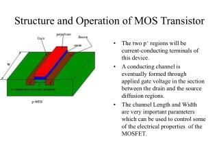
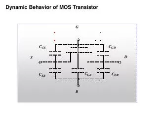
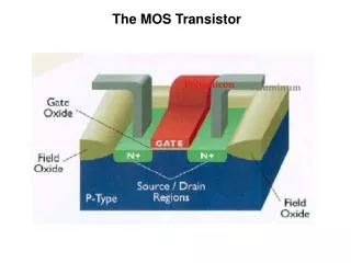
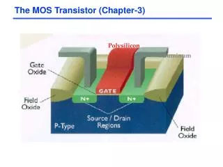
The MOS transistor is a majority carrier device having the current in the conducting channel being controlled by the voltage applied at the gate terminal. A pMOS has holes as majority carriers while an nMOS has electrons as majority carriers.

E N D
The MOS transistor is a majority carrier device having the current in the conducting channel being controlled by the voltage applied at the gate terminal. A pMOS has holes as majority carriers while an nMOS has electrons as majority carriers. A MOS structure with two terminals (no drain or source) can operate in three regions. These are: Accumulation Depletion and Inversion Of significance is interface at the parallel plate capacitor. MOS Transistor Theory
The Fermi Potential • The function of temperature and doping concentration that denotes the difference between the intrinsic Fermi Level Ei and the Fermi Level EF is the Fermi Potential. • It is given by:
The electron affinity of Silicon which is the potential difference between the conduction band and the vacuum (free space) is expressed as qχ. The energy required to move an electron from the Fermi Level into free space is called the work function qΦS and is given by: qΦS= qχ+EC-EF If we bring the gate material (poly), the silicon dioxide (SiO2) and the Semiconductor (Si) together, the Fermi Levels have to line up to form a MOS capacitor. The Fermi potential at the surface also called surface potential ΦS is smaller in magnitude than the bulk Fermi potential ΦF. If we apply an external voltage to the gate of the MOS capacitor when the bulk voltage is 0Vand depending on the polarity and magnitude of the applied voltage we end up with three regions of operation, namely accumulation, Depletion and inversion. IF a fairly small gate voltage (positive) is applied at the gate the region at the semiconductor/Oxide interface becomes devoid of mobile carriers. The Fermi Potential
The Depletion Region • The thickness of the depletion region xd can be computed as a function of the surface potential ΦS. • The amount of the depletion region charge plays an important role in the analysis of the threshold voltage. • The surface at the Semiconductor/Oxide interface is said to be inverted when the density of mobile electrons on the surface becomes equal to the density of holes in the bulk. • This condition dictates that