Download
1 / 34
710 likes | 1.39k Views
UNIT -1 Chapter -2. MOS TRANSISTOR THEORY. ( Neil weste p:- 41- 91). Introduction. A MOS transistor is a majority-carrier device , in which the current in a conducting channel between the source and the drain is modulated by a voltage applied to the gate. NMOS (n-type MOS transistor)

E N D
UNIT -1 Chapter -2 MOS TRANSISTOR THEORY (Neilwestep:- 41- 91)
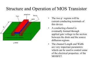
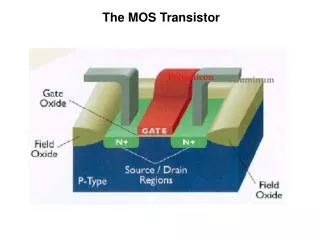
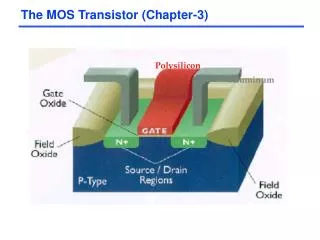
Introduction • A MOS transistor is a majority-carrier device, in which the current in a conducting channel between the source and the drain is modulated by a voltage applied to the gate.
NMOS (n-type MOS transistor) • Majority carrier = electrons • A positive voltage applied on the gate with respect to the substrate enhances the number of electrons in the channel and hence increases the conductivity of the channel. • If gate voltage is less than a threshold voltage Vt , the channel is cut-off (very low current between source & drain). • PMOS (p-type MOS transistor) • Majority carrier = holes • Applied voltage is negative with respect to substrate.
Relationship between Vgs and Ids, for a fixed Vds: n-channel enhancement n-channel depletion Ids Ids - Vt Vgs + Vt Vgs Vgs + Vt Vgs - Vt Ids Ids n-channel depletion p-channel enhancement
Devices that are normally cut-off with zero gate bias are classified as "enhancementmode"devices. • Devices that conduct with zero gate bias are called "depletion-mode"devices. • Enhancement-mode devices are more popular in practical use.
nMOS Enhancement Transistor • At Vds=+V, Vgs=0V, no current flows from source to drain because they are insulated by two reverse biased pn junction • Accumulation mode (Vgs << Vt) • Depletion mode (Vgs ≈ Vt) • Inversion mode (Vgs > Vt)
The factors that influence the level of drain current Ids (b/w S and D) • Distance b/w S and D • Channel width • Threshold voltage Vt • Thickness of SiO2 • Dielectric constant of insulator • Carrier mobility
Threshold voltage (Vt): • The voltage at which an MOS device begins to conduct ("turn on"). The threshold voltage is a function of (1) Gate conductor material (2) Gate insulator material (3) Gate insulator thickness (4) Impurity at the silicon-insulator interface (5) Voltage between the source and the substrate Vsb (6) Temperature
Vt,can be expressed as • Where Vt-mos is the ideal threshold voltage of an ideal transistor and Vfb is termed as flat-band voltage. Threshold voltage (Vt)equation
Effect due to series connection of transistors • Increases if source voltage increases because source is connected to the channel • Increase in Vt with Vs is called the body effect Body Effect
The cutoff region is also referred to as the subthreshold region. • The value of Ids is very small Sub threshold region
Mobility decreases with increasing doping concentration and increasing temperature. Average carrier drift velocity (V) Electric field (E) µ= Mobility variation
n n Electron Tunneling Gate Source Drain Poly Si SiO2 Thinox Substrate • When the gate oxide is very thin, a current can flow from gate to source or drain by electron tunneling through the gate oxide.
The drain is at a high enough voltage with respect to the source. Causes current to flow irrespective of the gate voltage. Drain punch through
n n Hot elections Gate Source Drain Poly Si SiO2 Thinox Substrate Due to excess Vds, hot electrons impact the drain, dislodging holes that are then swept toward the negatively charged substrate and appear as a substrate current. This effect is known as impact ionization
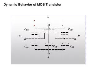
n n Small signal AC Characteristics Gate Source Drain SiO2 Thinox p Substrate Cgb Cgd Cgs Cdb Poly Si
Output conductance (gds) in the linear region can be obtained by differentiating linear equation. The transconductance expresses the relationship between output current ids and input voltage Vgs
VDD 1 0 Vin Vout CMOS invertors DC characteristics GND
Idsp Idsn -Vgsp1 -Vgsp2 -Vgsp3 Idsp -Vgsp4 Vgsn4 Vgsn3 Vgsn2 Vgsn1
A VDD C Vout D E VDD Vin
βn/βp Ratio A. βn/βp=10 B. βn/βp=1 C. βn/βp=0.1 C Vout B A Vin
Noise Margin • NML = VILmax-VOLmax • NMH = VOHmax-VLIHmin
Input /output transfer curve A B VDD C .5VDD Vout D E .5VDD VDD- VDD Vtn Vtp Vin
βn/βp Ratio • The ratio βn/βp is decreases the transition region shifts from left to right A. βn/βp=10 C B. βn/βp=1 Vout C. βn/βp=0.1 B A Vin
Noise Margin • Noise Margin:Determines the allowable noise voltage on the input of a gate so that the output will not be affect. • Noise Margin is in terms of two parameters LOW noise margin NML and HIGH noise margin NMH
NML is define as the difference in magnitude between the maximum LOWoutput voltage of the driving gate and the maximum input LOW voltage recognized by the driven gate. • NML = VILmax-VOLmax • NMH is define as the difference in magnitude between the minimum HIGH output voltage of the driving gate and the minimum input HIGH voltage recognized by the receiving gate. • NMH = VOHmax-VLIHmin
Static load MOS inverters • Apart from the CMOS inverter , there are many other forms of MOS inverter that may be used to build logic gates • Ex: resistive load inverter • If resister value increases transfer curve leads to left side.
The Pseudo-nMOS inverter • Pseudo inverter that uses a p-device pull-up or load that has its gate permanently grounded. • An n-device pull-down or driver is driven with the input signal. • βn/βp affects transfer characteristic • If nMOS on then Vout=
Saturated load inverter • An inverter design using nMOS transistor load. • But remember that the threshold is modified by the body effect because the source of the n-load transistor above Vss
n n Gate Source Drain Poly Si SiO2 Thinox ThnQ Substrate